
Pixel structure and manufacturing method of pixel structure
A pixel structure and manufacturing method technology, which is applied in semiconductor/solid-state device manufacturing, electrical components, transistors, etc., can solve the problems of reducing the display aperture ratio of the pixel structure and increasing the area of the metal pattern, and achieve the effect of increasing the display aperture ratio
Patent Information
- Authority / Receiving Office
- CN · China
- Patent Type
- Patents(China)
- Current Assignee / Owner
- Publication Date
- 2016-03-02
Smart Images
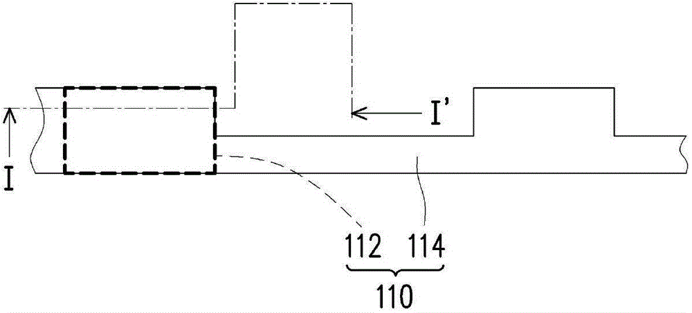
Figure 1 
Figure 2 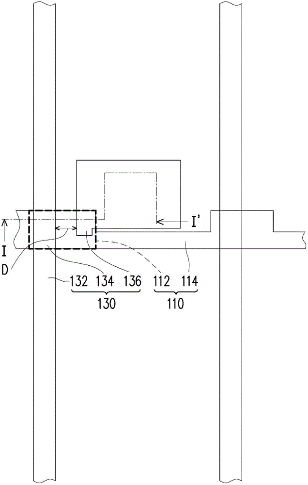
Figure 3
Abstract
Description
technical field
[0001] The present invention relates to a pixel structure and its manufacturing method, and in particular to a high aperture ratio pixel structure and its manufacturing method. Background technique
[0002] Currently common flat panel displays use a pixel structure to constitute the smallest basic unit required for displaying images, wherein the pixel structure roughly includes an active element and a pixel electrode. Generally speaking, when the active element in a specific pixel structure is turned on through the corresponding scan line, the operating voltage provided by the data line can be input to the pixel electrode through the active element to display the corresponding display data. In addition, the pixel structure also includes a storage capacitor (storage capacitor), so that the pixel structure has a voltage holding function. That is, the storage capacitor is used to store the operating voltage input to the pixel electrode through the active elemen...
Examples
Embodiment Construction
[0039] Figure 1A to Figure 6A It is a schematic top view of the components produced in each step of the method for fabricating the pixel structure according to an embodiment of the present invention, and Figure 1B to Figure 6B respectively Figure 1A to Figure 6A Schematic cross-sectional view along line I-I'. Please refer to Figure 1A and Figure 1B A method for fabricating a pixel structure according to an embodiment of the present invention includes fabricating a patterned conductor layer 110 on a substrate 10 to form a gate 112 to be connected to a scan line 114 . Specifically, the gate 112 formed by the patterned conductive layer 110 and the scan line 114 are formed by a continuous pattern, so the gate 112 can be regarded as a part of the scan line 114 . However, in other embodiments, the patterned conductor layer 110 may include a linear pattern with a fixed line width and a branch pattern connected to the linear pattern, wherein the scan line 114 may be formed by s...