
pixel structure
A pixel structure and pixel electrode technology, applied in instruments, nonlinear optics, optics, etc., can solve problems such as color shift and viewing angle, achieve wide viewing angle display effect, increase display aperture ratio, improve color shift phenomenon and viewing angle problems. Effect
Patent Information
- Authority / Receiving Office
- CN · China
- Patent Type
- Patents(China)
- Current Assignee / Owner
- Publication Date
- 2020-12-25
Smart Images
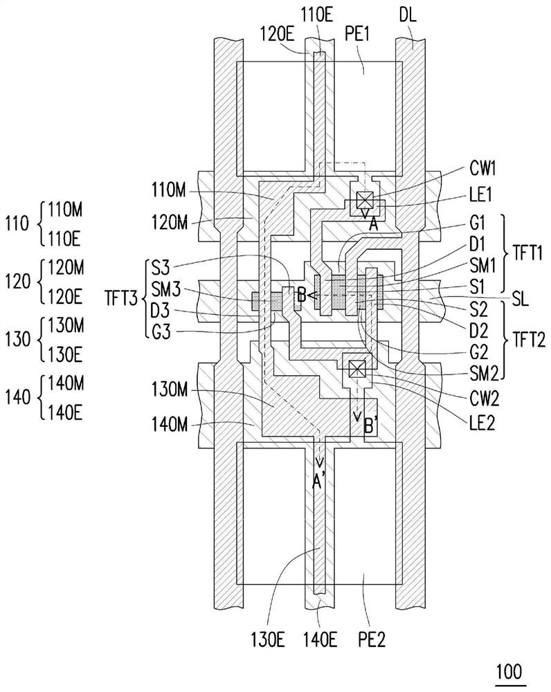
Figure 1 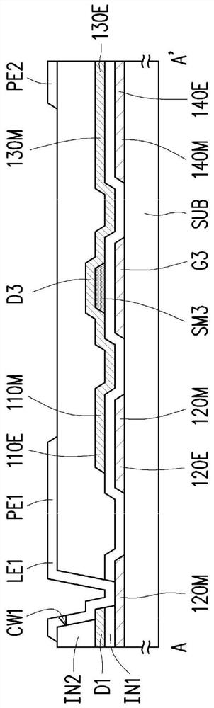
Figure 2 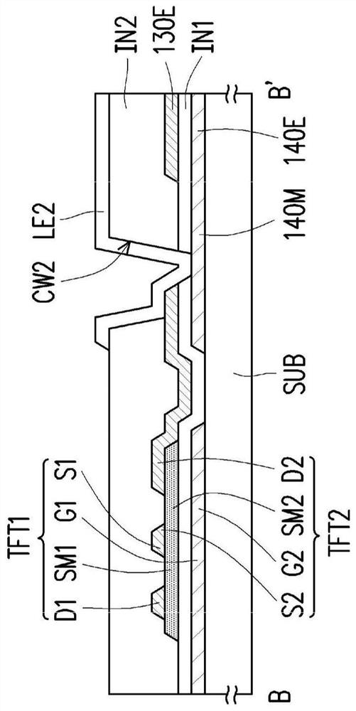
Figure 3
Abstract
Description
technical field
[0001] The present invention relates to the field of display technology, in particular, to a pixel structure with capacitance. Background technique
[0002] With the advancement of optoelectronic and semiconductor technologies, it drives the vigorous development of flat panel displays. Among many flat-panel displays, liquid crystal displays have become the mainstream in the market because of their superior characteristics such as high space utilization efficiency, low power consumption, no radiation, and low electromagnetic interference. At present, liquid crystal displays usually have a wide viewing angle when displaying images, so as to meet the needs of multiple users viewing the same display device at the same time. However, the phenomenon of color washout in displays with wide viewing angles is also criticized by people. In order to solve the problem of color shift, the design of the pixel structure in the prior art reduces the aperture ratio of the di...
Examples
Embodiment Construction
[0061] figure 1 It is a schematic top view of a pixel structure according to an embodiment of the present invention. figure 2 yes figure 1 The schematic cross-sectional view of the pixel structure along the section line A-A'. image 3 yes figure 1 The schematic cross-sectional view of the pixel structure along the section line B-B'. For clarity and ease of explanation, figure 1 Partial film layers are omitted. Below, will pass Figure 1 to Figure 3 An embodiment of the present invention will be described in detail.
[0062] The pixel structure 100 includes a first active element TFT1, a first pixel electrode PE1, a first capacitor electrode 110, a second capacitor electrode 120, a second active element TFT2, a second pixel electrode PE2, a third capacitor electrode 130, and a fourth capacitor electrode 140 and the third active element TFT3. In some embodiments, the pixel structure 100 further includes a scan line SL, a data line DL, a first insulating layer IN1, a sec...