
pixel structure
A technology of pixel structure and pixel electrode, which is applied in the field of pixel structure, can solve the problems of color shift, image residue, etc., and achieve the effect of solving color shift and image residue
Patent Information
- Authority / Receiving Office
- CN · China
- Patent Type
- Patents(China)
- Current Assignee / Owner
- Publication Date
- 2019-03-08
Smart Images
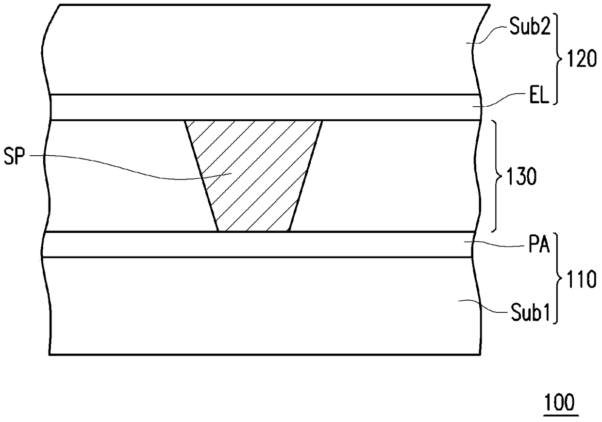
Figure 1 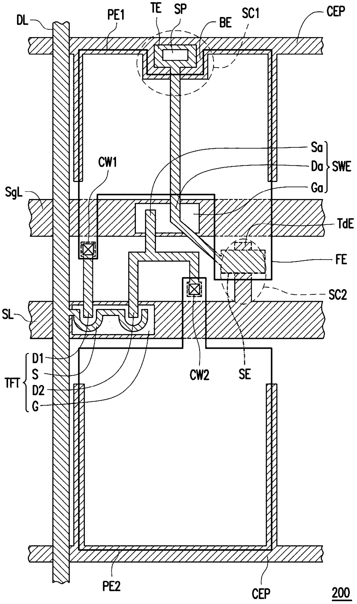
Figure 2 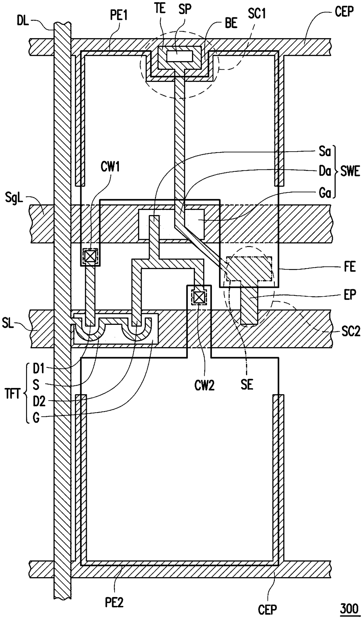
Figure 3
Abstract
Description
technical field
[0001] The present invention relates to a pixel structure, and in particular to a pixel structure of a display panel. Background technique
[0002] With the advancement of optoelectronic and semiconductor technologies, it drives the vigorous development of flat panel displays. Among many flat-panel displays, liquid crystal displays have become the mainstream in the market because of their superior characteristics such as high space utilization efficiency, low power consumption, no radiation, and low electromagnetic interference. At present, liquid crystal displays usually have a wide viewing angle when displaying images, so as to meet the needs of multiple users viewing the same display device at the same time. However, the phenomenon of color washout in displays with wide viewing angles is also criticized by people. In order to solve the problem of color shift, the design of the pixel structure in the prior art will reduce the aperture ratio of the display...
Examples
Embodiment Construction
[0043] figure 1 It is a schematic cross-sectional view of a display panel according to an embodiment of the present invention. Please refer to figure 1 , the display panel 100 includes a pixel array substrate 110 , an opposite substrate 120 and a display medium 130 . The display panel 100 is, for example, a liquid crystal display panel or other types of display panels.
[0044] The pixel array substrate 110 includes a substrate sub1 and a pixel array PA. The material of the substrate sub1 can be glass, quartz, organic polymer or metal and so on. The pixel array PA is configured on the substrate sub1, and the pixel array PA includes a plurality of pixel structures. The design of the pixel structure will be described in detail later.
[0045] The opposite substrate 120 is located on the opposite side of the pixel array substrate 110 . The counter substrate 120 includes a substrate sub2 and an electrode layer EL. The material of the substrate sub2 can be glass, quartz or o...