
A charge pump circuit
A technology of charge pump and circuit, applied in the direction of conversion equipment without intermediate conversion to AC, can solve the problem of high cost
Patent Information
- Authority / Receiving Office
- CN · China
- Patent Type
- Patents(China)
- Current Assignee / Owner
- Publication Date
- 2015-12-09
Smart Images
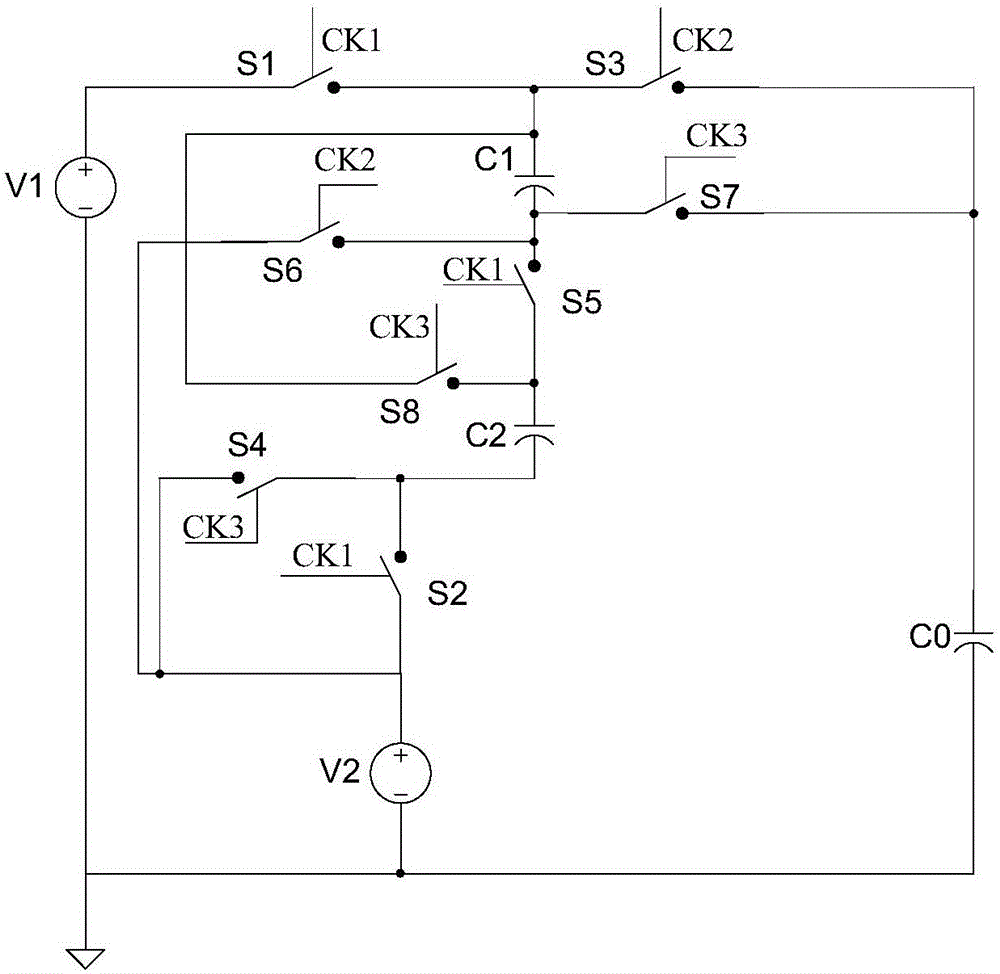
Figure 1 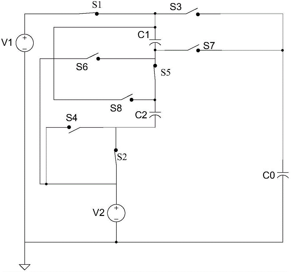
Figure 2 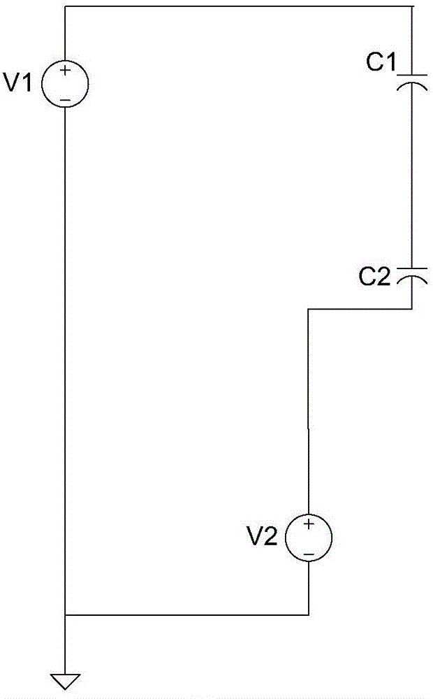
Figure 3
Abstract
Description
technical field
[0001] The invention relates to the technical field of voltage conversion, in particular to a charge pump circuit. Background technique
[0002] There are two common charge pumps in the prior art: one is used in a phase-locked loop circuit and is connected to the rear stage of a frequency and phase detector to generate a relatively stable voltage by charging and discharging a capacitor for use in Control the frequency of the voltage-controlled oscillator; the other is through the switch capacitor, which is used for voltage conversion and can provide a power output circuit with a large output current. Because this charge pump can achieve high voltage conversion efficiency, it is based on the switch capacitor The charge circuit is widely used in voltage conversion circuits. In order to distinguish the two, the latter is called a power charge pump. A general power charge pump adopts an input voltage and can generate an output voltage higher than the input volt...
Examples
Embodiment Construction
[0035] The specific embodiments of the present invention will be described in detail below in conjunction with the accompanying drawings. It should be noted that these specific descriptions are only for those of ordinary skill in the art to understand the present invention more easily and clearly, rather than limiting interpretation of the present invention.
[0036] Such as figure 1 Shown is the structural diagram of the charge pump circuit provided by the present invention. The charge pump circuit provided by the invention includes: two power supplies, eight switches, three capacitors and three clock signals. specifically:
[0037] The charge pump circuit includes: a first input power supply V1; a first capacitor C1; a second capacitor C2; an output capacitor C0; it is characterized in that it also includes:
[0038] The second input power supply V2, one end of which is connected to an equipotential point with one end of the first input power supply V1, and one end of the ...