
A fast recovery diode and its manufacturing method
A technique for recovering diodes and manufacturing methods, which is applied in semiconductor/solid-state device manufacturing, electrical components, circuits, etc., which can solve problems such as hidden circuit failure, slow recovery speed, and device characteristic degradation, and reduce the amount of hole injection in the P region , The effect of reducing the number of injected holes and reducing the surface concentration
Patent Information
- Authority / Receiving Office
- CN · China
- Patent Type
- Patents(China)
- Current Assignee / Owner
- Publication Date
- 2017-02-01
Smart Images
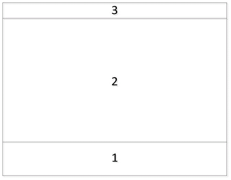
Figure 1 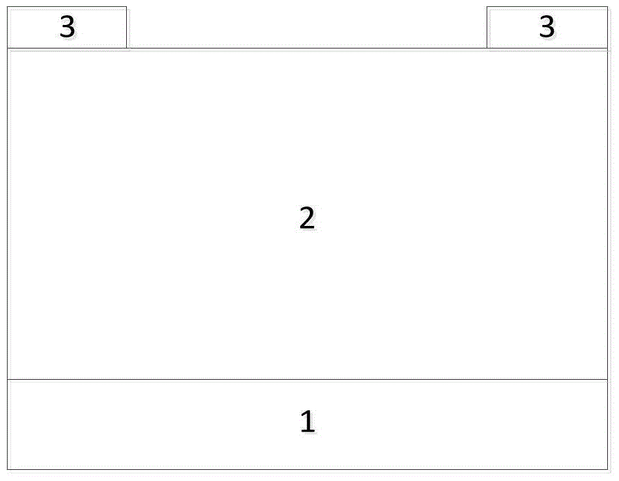
Figure 2 
Figure 3
Abstract
Description
technical field
[0001] The invention relates to a power semiconductor device and a manufacturing method thereof, in particular to a fast recovery diode and a manufacturing method thereof. Background technique
[0002] When a PIN diode conducts forward current, it generally injects a large number of carriers from the anode (P region) and cathode (N+ region) to the drift region (I region), and the hole carriers injected from the anode form a minority in the drift region. store charge in the form of . The minority carrier injection causes the conductance modulation effect in the drift region, thereby reducing the forward on-state voltage drop, which is the biggest advantage of both PIN diodes and bipolar devices. When a reverse voltage is suddenly applied to the conducting diode, the device will not be turned off immediately because a large number of minority carriers are stored in the drift region during conduction. Only when these minority carriers are completely extracted ...
Examples
Embodiment Construction
[0033] The specific implementation manners of the present invention will be further described in detail below in conjunction with the accompanying drawings.
[0034] Aiming at the technical problems existing in the prior art, the present invention provides a fast recovery diode and its manufacturing method. The present invention reduces the holes injected into the N-region (i.e., I-region) from the P region while ensuring the concentration on both sides of the PN junction structurally. Quantity, so that sufficient speed can be achieved through fewer recombination centers, and on the basis of ensuring the working characteristics of the device, the dependence of the device on the lifetime control technology is reduced. At the same time, the number of holes participating in the conductance modulation decreases, making the temperature coefficient of the voltage drop tend to zero, making it easier to connect in parallel.
[0035] The fast recovery diode includes a substrate and a P...