
A kind of preparation method of power diode
A technology of power diodes and silicon dioxide, applied in semiconductor/solid-state device manufacturing, electrical components, circuits, etc., can solve the problems of high cost, time-consuming, low efficiency, etc., to improve the withstand voltage level and reduce the forward turn-on voltage, the effect of improving the withstand voltage of the device
Patent Information
- Authority / Receiving Office
- CN · China
- Patent Type
- Patents(China)
- Current Assignee / Owner
- Publication Date
- 2017-05-17
Smart Images
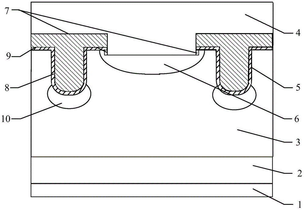
Figure 1 
Figure 2 
Figure 3
Abstract
Description
technical field
[0001] The invention relates to a method for preparing a power diode, which belongs to the technical field of semiconductor manufacturing. Background technique
[0002] Traditional rectifier diodes mainly include PN junction diodes and Schottky diodes. The PN junction diode has a large forward voltage drop VF and a long reverse recovery time Trr, but the PN junction diode has good stability and can work at high voltage; Schottky diodes are made of precious metals (such as gold, silver, titanium, etc. ) is in contact with the semiconductor to form a semiconductor device made of a heterojunction barrier, which has absolute advantages at low voltage: its forward voltage drop is small, the reverse recovery time is short, and it has a wide range of applications in high-speed fields. However, Schottky diodes have the following disadvantages:
[0003] 1. The reverse leakage current is relatively high and unstable. In particular, its leakage current will increase ...
Examples
Embodiment Construction
[0048] The principles and features of the present invention are described below in conjunction with the accompanying drawings, and the examples given are only used to explain the present invention, and are not intended to limit the scope of the present invention.
[0049] Such as figure 1 As shown, a power diode according to the present invention comprises a bottom electrode 1, a substrate layer 2, an N-type epitaxial layer 3 and a top electrode 4 from bottom to top, the top electrode 4 is the anode of the power diode, and the bottom electrode 1 is the negative pole of the power diode; wherein at least two grooves 5 are arranged laterally on the upper part of the N-type epitaxial layer 3, and between the N-type epitaxial layer 3 and the top electrode 4 between two adjacent grooves 5 pbody area 6;
[0050] The cross-section of the pbody region 6 is in a "concave" shape with an arc at the bottom, wherein the two convex parts on the upper part of the "concave" shape are the edge...