
Schottky diode
A Schottky diode and Schottky contact technology, applied in electrical components, circuits, semiconductor devices, etc., can solve the problems of limited high voltage withstand capability, high reverse bias voltage, and inability to provide, to achieve improved withstand voltage capability, Effects of high reverse withstand voltage capability and low on-state power consumption
Patent Information
- Authority / Receiving Office
- CN · China
- Current Assignee / Owner
- Publication Date
- 2013-04-10
- Estimated Expiration
- Not applicable · inactive patent
Smart Images
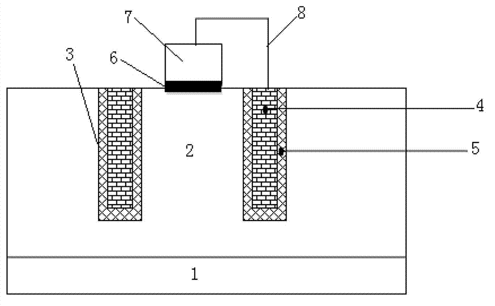
Figure 1
Abstract
Description
technical field
[0001] The invention relates to the field of semiconductor manufacturing, in particular to a Schottky diode. Background technique
[0002] The traditional PN junction diode is in a single crystal semiconductor, part of which is doped with acceptor impurities is P-type semiconductor, and the other part is doped with donor impurities is N-type semiconductor, and the transition near the interface between P-type semiconductor and N-type semiconductor The region is called a PN junction, and a space charge layer is formed on both sides of its interface, and a self-built electric field is built. When there is no applied voltage, the diffusion current caused by the carrier concentration difference on both sides of the PN junction is equal to the drift current caused by the self-built electric field, and is in a state of electrical balance; when there is a forward voltage bias outside, the external electric field and the self-built electric field The mutual suppressi...
Examples
Embodiment Construction
[0023] Such as figure 1 As shown, the Schottky diode of the present invention includes: an N-type epitaxial 2 on an N-type substrate 1, a deep trench 3 in the N-type epitaxial 2, a silicon dioxide layer 4 in the deep trench 3, and a deep trench There is a polysilicon region 5 inside the silicon dioxide layer 4 in the trench 3, a Schottky contact region 6 above the N-type epitaxy 2 between the deep trenches 3, a metal layer 7 on the Schottky contact region 6, and a polysilicon region 5 and the metal layer 7 are connected by a metal wire 8, wherein the thickness of the silicon dioxide layer 4 is greater than 1000 angstroms, the depth of the deep trench 3 is greater than 4um, and the metal layer is titanium metal.
[0024] With the increase of the thickness of the silicon dioxide layer 4, the withstand voltage capability of the present invention increases accordingly, and the ratio of the thickness of the silicon dioxide layer to the withstand voltage capability of the present in...