
Electrostatic discharge protection structure in semiconductor device and semiconductor device
An electrostatic discharge protection, semiconductor technology, applied in the direction of semiconductor devices, semiconductor/solid-state device components, electric solid-state devices, etc., can solve the problems of small withstand current, burnout of protective structure, etc., to achieve increased withstand current, reduced Rdson, On-resistance reduction effect
Patent Information
- Authority / Receiving Office
- CN · China
- Patent Type
- Patents(China)
- Current Assignee / Owner
- Publication Date
- 2017-12-15
Smart Images
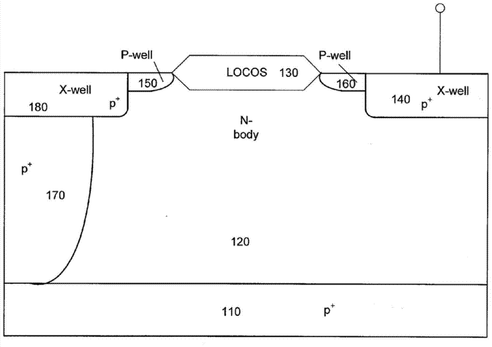
Figure 1 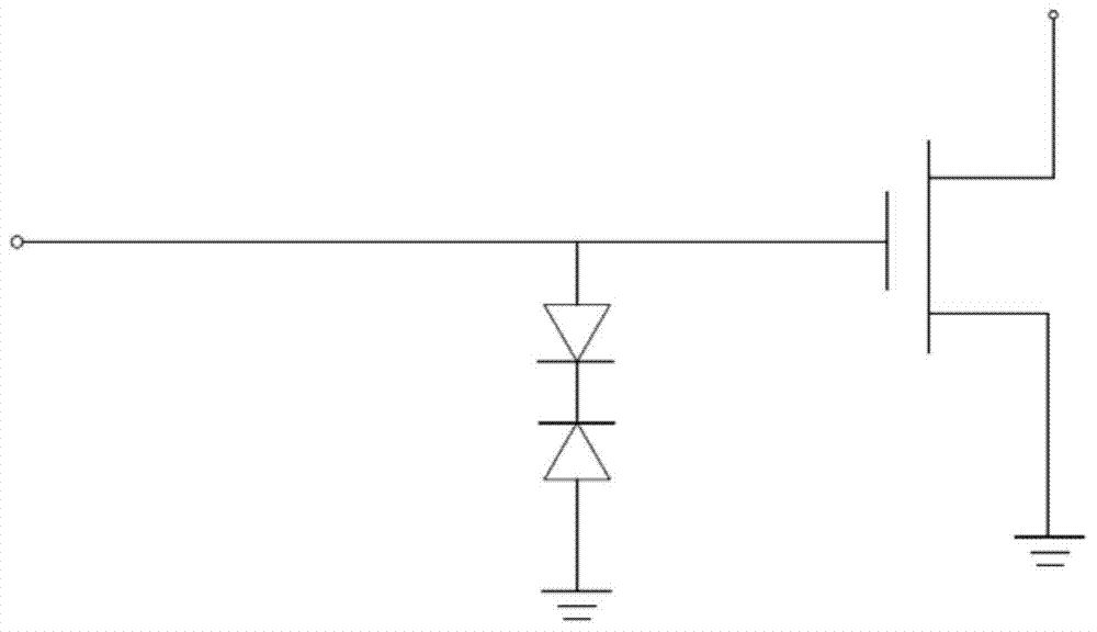
Figure 2 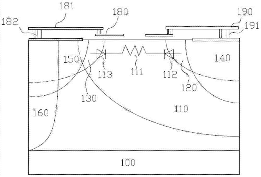
Figure 3
Abstract
Description
technical field
[0001] The invention belongs to the field of semiconductor device production, in particular to a semiconductor device with an electrostatic protection structure. Background technique
[0002] Static electricity exists all the time in nature. When the external environment of the chip or the static charge accumulated inside the chip flows into or out of the chip through the pins of the chip, the instantaneous current (peak value can reach several amperes) or voltage will damage the integrated circuit. circuit, making the chip function invalid. With the development of the semiconductor industry, the feature size is further reduced, the component density is increasing, and the electronic components are more likely to suffer from electrostatic damage. Industrial electronic devices must be designed with qualified electrostatic protection.
[0003] Among power amplifier devices, high-power devices such as VDMOS, LDMOS, and IGBT can withstand high voltage, and the m...
Examples
Embodiment Construction
[0029] As mentioned in the background art, an existing ESD protection structure of a semiconductor device is realized by arranging a pair of back-to-back diodes. The working principle of this ESD protection structure is that when the externally applied voltage is greater than the breakdown voltage of one of the diodes, the ESD protection structure works in a conduction mode, and the external voltage is derived from the branch where the ESD protection structure is located. In this case, the breakdown voltage of each diode is proportional to the on-resistance Rdson when the structure turns on. In order to achieve the protection voltage required by the device, in the prior art, a thick field oxide layer is formed between the two P-well regions to increase the resistance value of Rdson, thereby increasing the breakdown voltage. However, this method of increasing the on-resistance will reduce the withstand current of the EDS protection structure, causing the ESD protection structur...