
A kind of manufacturing method of n-type IBC silicon solar cell based on ion implantation process
A silicon solar cell and ion implantation technology, applied in the field of solar cells, can solve problems such as low boron content, and achieve the effects of high minority carrier lifetime, technical precision, and reduced recombination rate
Patent Information
- Authority / Receiving Office
- CN · China
- Patent Type
- Patents(China)
- Current Assignee / Owner
- Publication Date
- 2016-08-24
- Estimated Expiration
- Not applicable · inactive patent
Smart Images
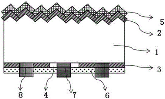
Figure 1
Abstract
Description
technical field
[0001] The invention belongs to the technical field of solar cells, and in particular relates to a manufacturing method of an n-type IBC silicon solar cell based on an ion implantation process. Background technique
[0002] Solar cells can directly convert solar energy into electrical energy, which is an effective way to utilize solar energy resources. Since no harmful substances are produced during use, solar cells are favored in solving energy and environmental problems and have a good market prospect. Solar energy is also Known as the most ideal energy source, it is an important resource for the survival and development of human society.
[0003] At present, the mainstream solar cell material uses p-type silicon as the substrate, and forms a pn junction through high-temperature phosphorus diffusion. For p-type silicon materials, because it is insensitive to metal impurities and many non-metal defects, and has fewer boron-oxygen pairs in the body, its perf...
Examples
Embodiment 1
[0036] This embodiment includes the following steps:
[0037] 1. Select an n-type silicon substrate with a resistivity of 3-5Ω·cm, and its minority carrier lifetime is greater than 500us, use chemical etching to remove the damaged layer on the surface of the silicon wafer, and make texture on both sides.
[0038] 2. Double-sided phosphorus diffusion: the diffusion resistance is 60Ω / □.
[0039] 3. Print corrosive paste on the p+ defined area on the back to remove the phosphosilicate glass in the p+ defined area.
[0040] 4. Use 20% TMAH solution to carry out selective etching at 60°C, polish the p+ defined area, and etch for 30 minutes.
[0041] 5. Remove the phosphosilicate glass on the front surface of the n-type silicon substrate, and use hydrofluoric acid, nitric acid and water with a volume ratio of 1:30:300 to etch the front surface of the n-type silicon substrate. 140Ω / □.
[0042] 6. Remove the back phosphosilicate glass and perform RCA cleaning.
[0043] 7. Using th...
Embodiment 2
[0050] This embodiment includes the following steps:
[0051] 1. Select an N-type silicon substrate with a resistivity of 5-12Ω·cm, whose minority carrier lifetime is greater than 500us, remove the damaged layer on the surface of the silicon wafer by chemical etching, and make texture on both sides.
[0052] 2. Double-sided phosphorus diffusion: the diffusion resistance is 80Ω / □.
[0053] 3. Use laser to remove the phosphosilicate glass in the p+ defined area.
[0054]4. Use 25% TMAH solution to carry out selective etching at 70°C, and polish the p+ defined area, and the etching time is 20 minutes.
[0055] 5. Remove the phosphosilicate glass on the front surface of the n-type silicon substrate, use 1:30:300 hydrofluoric acid, nitric acid and water to etch the front surface of the n-type silicon substrate at 25°C, and the etching time is 20min. The square resistance of the front surface after etching was 130Ω / □.
[0056] 6. Remove the back phosphosilicate glass and perform ...