
Organic electroluminescence device and preparation method thereof
An electroluminescence device and luminescence technology, which is applied in the direction of electric solid-state devices, semiconductor/solid-state device manufacturing, electrical components, etc., can solve the problems of poor refractive index, loss of total reflection, low light extraction performance, etc., and achieve stable luminous color, The effect of reducing the decay speed and reducing the potential barrier
Patent Information
- Authority / Receiving Office
- CN · China
- Patent Type
- Applications(China)
- Current Assignee / Owner
- Publication Date
- 2015-05-27
- Estimated Expiration
- Not applicable · inactive patent
Smart Images
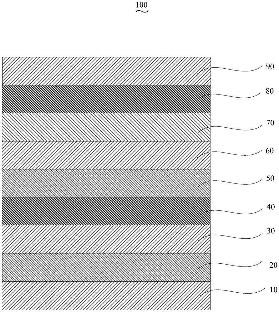
Figure 1 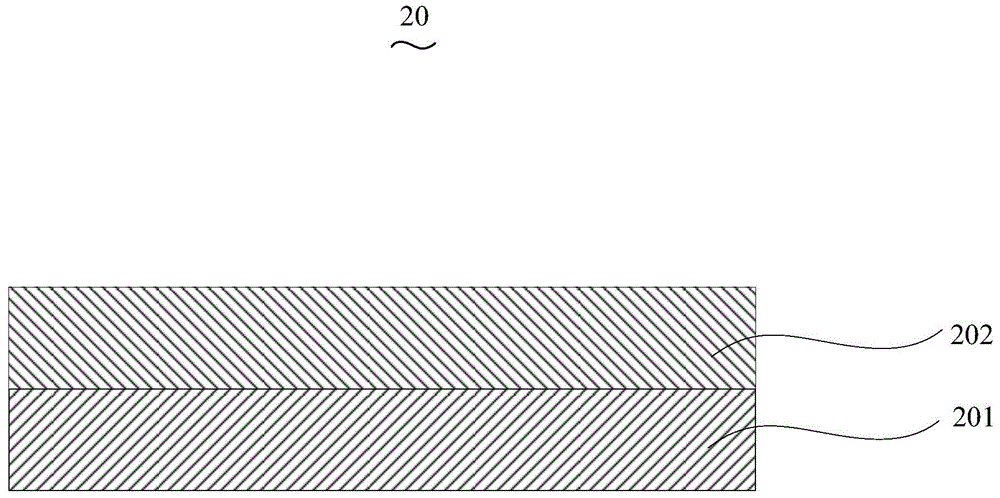
Figure 2 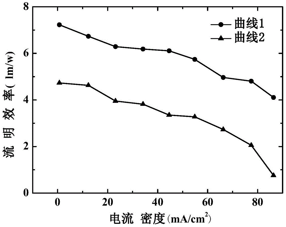
Figure 3
Abstract
Description
technical field
[0001] The invention relates to an organic electroluminescence device and a preparation method thereof. Background technique
[0002] The luminescence principle of organic electroluminescent devices is based on the action of an external electric field, electrons are injected from the cathode to the lowest unoccupied molecular orbital (LUMO) of organic matter, and holes are injected from the anode to the highest occupied molecular orbital (HOMO) of organic matter. Electrons and holes meet, recombine, and form excitons in the light-emitting layer. Excitons migrate under the action of an electric field, transfer energy to the light-emitting material, and excite electrons to transition from the ground state to the excited state. The excited state energy is deactivated by radiation to generate photons , releasing light energy.
[0003] In traditional light-emitting devices, only about 18% of the light inside the device can be emitted to the outside, while the res...
Examples
preparation example Construction
[0037] The preparation method of the organic electroluminescence device 100 of an embodiment, it comprises the following steps:
[0038] Step S110 , preparing the scattering layer 20 on the surface of the glass substrate 10 by electron beam evaporation.
[0039] The scattering layer 20 is formed on one side surface of the glass substrate 10 . The scattering layer 20 is composed of a luminescent material layer 201 and a binary doped layer 202. The luminescent material layer 201 is prepared on the surface of the glass substrate 10 by thermal resistance evaporation, and the material of the luminescent material layer 201 is selected from 4-(dinitrile Methyl)-2-butyl-6-(1,1,7,7-tetramethyljulonedine-9-vinyl)-4H-pyran (DCJTB), 9,10-di-β- Naphthalene anthracene (ADN), 4,4'-bis(9-ethyl-3-carbazolevinyl)-1,1'-biphenyl (BCzVBi) and 8-hydroxyquinoline aluminum (Alq 3 ), the binary doped layer 202 is prepared on the surface of the luminescent material layer 201 by electron beam evaporat...
Embodiment 1
[0059] The structure prepared in this example is glass substrate / Alq 3 / CaO:Re 2 o 7 / ITO / MoO 3 / NPB / Alq 3 / TAZ / CsF / Ag organic electroluminescent device, in this embodiment and the following embodiments, " / " indicates a layer, and ":" indicates doping.
[0060] The glass substrate is N-LASF44. After rinsing the glass substrate with distilled water and ethanol, soak it in isopropanol for one night. Prepare the scattering layer on the glass substrate. The scattering layer is composed of a luminescent material layer and a binary doping layer. The luminescent material layer is prepared by thermal resistance evaporation on the surface of the glass substrate. The material is Alq 3 , the thickness is 12nm, and the binary doped layer is prepared by electron beam evaporation on the surface of the luminescent material layer, and the material is CaO:Re 2 o 7 , CaO and Re 2o 7 The mass ratio is 5:1 and the thickness is 150nm. Then ITO is prepared on the scattering layer with a th...
Embodiment 2
[0068] The structure prepared in this example is glass substrate / DCJTB / CaCl 2 :ReO 2 / IZO / MoO 3 / NPB / ADN / TAZ / Cs 2 CO 3 / Au organic electroluminescent devices.
[0069] The glass substrate is N-LAF36. After rinsing the glass substrate with distilled water and ethanol, soak it in isopropanol for one night to prepare a scattering layer on the glass substrate. The scattering layer is composed of a luminescent material layer and a binary doping layer. The luminescent material layer is prepared by thermal resistance evaporation on the surface of the glass substrate. The material is DCJTB with a thickness of 50nm. The binary doped layer is prepared by electron beam evaporation on the surface of the luminescent material layer. The material is CaCl 2 :ReO 2 , CaCl 2 with ReO 2 The mass ratio is 4:1 and the thickness is 300nm. Then IZO is prepared on the scattering layer with a thickness of 80nm, which is prepared by magnetron sputtering; the hole injection layer is evaporated, ...