
Photo-alignment method, liquid crystal display panel and preparing method thereof
A liquid crystal display panel, photo-alignment technology, applied in optics, nonlinear optics, instruments, etc., can solve problems affecting pixel aperture ratio, transmittance bottlenecks, etc., and achieve the effect of reducing dark lines and improving transmittance.
Patent Information
- Authority / Receiving Office
- CN · China
- Current Assignee / Owner
- Publication Date
- 2017-03-15
- Estimated Expiration
- Not applicable · inactive patent
Smart Images
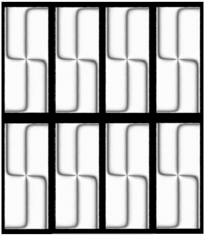
Figure 1 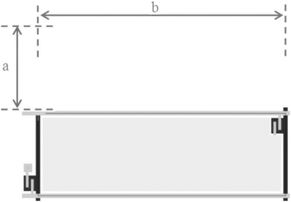
Figure 2 
Figure 3
Abstract
Description
technical field
[0001] The invention belongs to the technical field of manufacturing liquid crystal display panels, and in particular relates to an optical alignment method, a liquid crystal display panel and a manufacturing method thereof. Background technique
[0002] In the TFT-LCD production process, there are two liquid crystal alignment methods: rubbing alignment and photo alignment. Rubbing alignment can generate static electricity and particle contamination. Photo-alignment is a non-contact alignment technology that uses linearly polarized light to irradiate the light-sensitive polymer alignment film to form a tilt angle on the polymer alignment film.
[0003] In traditional pixel design, light alignment will form "swastika dark pattern" or "swastika dark pattern" inside the pixel, collectively referred to as swastika dark pattern, such as figure 1 shown. Swastika pattern seriously affects the aperture ratio of pixels, especially as the number of pixels per inch o...
Examples
Embodiment Construction
[0032] The implementation of the present invention will be described in detail below in conjunction with the accompanying drawings and examples, so as to fully understand and implement the process of how to apply technical means to solve technical problems and achieve technical effects in the present invention. It should be noted that, as long as there is no conflict, each embodiment and each feature in each embodiment of the present invention can be combined with each other, and the formed technical solutions are all within the protection scope of the present invention.
[0033] Such as figure 2 Shown is a schematic top view of a rectangular pixel, whose long side is b and wide side is a. In the traditional photoalignment mode pair figure 2 When the pixels shown are aligned, the TFT side (that is, the array substrate side) is exposed and aligned up and down along the long side of the pixel, and the exposure width is half of the wide side of the corresponding pixel, that is...