
Semiconductor component overturning device and test equipment thereof
A test equipment, semiconductor technology, applied in semiconductor/solid-state device manufacturing, electrical components, conveyor objects, etc., can solve the problem that semiconductor components cannot be picked and placed at the same time
Patent Information
- Authority / Receiving Office
- CN · China
- Current Assignee / Owner
- Publication Date
- 2017-05-31
- Estimated Expiration
- Not applicable · inactive patent
Smart Images
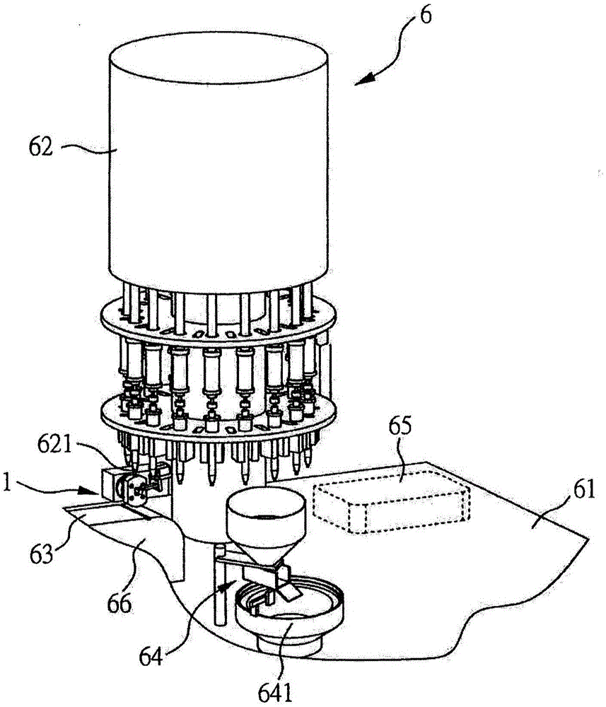
Figure 1 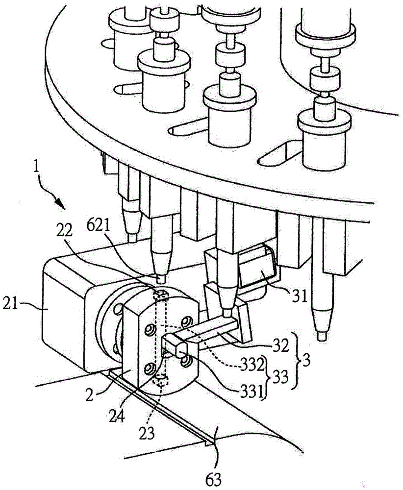
Figure 2 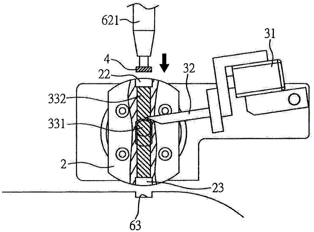
Figure 3
Abstract
Description
technical field
[0001] The invention relates to a semiconductor element inversion device and its testing equipment, especially to a semiconductor element inversion device and its testing equipment suitable for front and back conversion. Background technique
[0002] Known technologies such as the semiconductor element flipping device and method disclosed in Taiwan Patent Publication No. I462240, please refer to Figure 13 , is a continuous operation diagram of a known semiconductor element flipping device. As shown in the figure, the openable first platform 930 and the second platform 932 are connected by a turning shaft 928. The turning shaft 928 includes a first shaft and a second shaft which are coaxial and can rotate separately or simultaneously. The first carrier 934 has a plurality of trays 924 carrying semiconductor components, and the second carrier 938 has the same number of trays 924 not carrying semiconductor components. After the first platform 930 and the secon...
Examples
Embodiment Construction
[0023] see figure 1 and figure 2 , is a perspective view of the semiconductor element inversion testing equipment and a perspective view of the semiconductor element inversion device according to the first embodiment of the present invention. Such as figure 1 As shown, first viewed from the whole, the semiconductor device inversion testing equipment of the present invention includes a semiconductor device inversion device 1 and a sorting machine 6 . In this embodiment, the sorting machine 6 includes a turret 62 arranged on a working table 61 and a feeding area 64, a testing area 65 and a discharging area 66 arranged around the turret 62, wherein The material area 64 can be a vibrating plate (Bowl feeder) 641 , and the output area 66 includes a packaging roll 63 . The turret 62 includes a plurality of suction heads 621 arranged at intervals at an angle, one end of which sucks a semiconductor element 4 from the feed area 64 and rotates to the test area 65, and then turns t...