
Touch substrate and preparation method thereof and touch panel
A substrate and touch technology, applied in the direction of instruments, electrical digital data processing, data processing input/output process, etc., can solve the problem of high incidence of dark line defects, reduce the incidence of dark line defects, have little impact, and facilitate The effect of implementation
Patent Information
- Authority / Receiving Office
- CN · China
- Patent Type
- Applications(China)
- Current Assignee / Owner
- Publication Date
- 2018-05-22
Smart Images
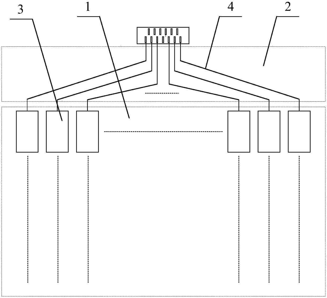
Figure 1 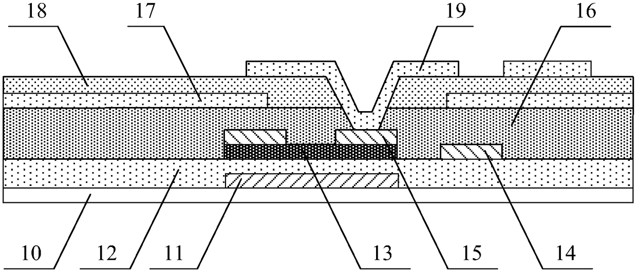
Figure 2 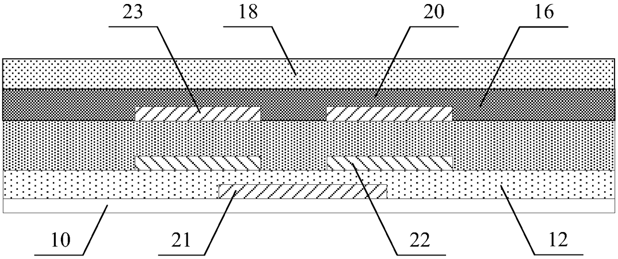
Figure 3
Abstract
Description
technical field
[0001] The invention relates to the field of display technology, in particular to a touch substrate, a preparation method thereof, and a touch panel. Background technique
[0002] With the rapid development of display technology, touch screen panels (Touch Screen Panels) have gradually spread in people's lives. At present, the touch panels can be classified into Add on Mode, OnCell, In Cell, etc. according to the structure. Among them, the plug-in touch panel is produced separately from the touch module and the display module, and then bonded together to form a touch panel with touch function, which has disadvantages such as high production cost, low light transmittance, and thick module. . The in-cell touch panel is to embed the touch electrodes of the touch module inside the display module, combining the display and touch control into one, which not only makes the product thinner and lighter, but also lowers the cost.
[0003] At present, there are three...
Examples
no. 1 example
[0057] Figure 2A It is a schematic structural diagram of the display area of the first embodiment of the touch substrate of the present invention, Figure 2B It is a schematic structural diagram of the fan-out area of the first embodiment of the touch substrate of the present invention. Such as Figure 2A As shown, the display area of the touch control substrate includes: a gate electrode 11 disposed on a substrate 10, a first insulating layer 12 covering the gate electrode 11, an active layer 13 and a signal line 14 disposed on the first insulating layer 12, The source and drain electrodes 15 arranged on the active layer 13, the second insulating layer 16 covering the active layer 13, the signal line 14 and the source and drain electrodes 15, the touch electrode 17 arranged on the second insulating layer 16, covering the touch The third insulating layer 18 of the control electrode 17 and the pixel electrode 19 disposed on the third insulating layer 18 . Wherein, the...
no. 2 example
[0076] Figure 13 It is a schematic structural diagram of the second embodiment of the touch substrate of the present invention, illustrating the structure of the fan-out area. Such as Figure 13 As shown, this embodiment is a modification of the scheme of the aforementioned first embodiment, the structure of the display area is the same as that of the first embodiment, the difference is that the protective layer 20 set in the fan-out area is set on the third insulating layer 18 . Specifically, the fan-out area of the touch substrate includes: the gate lead-out line 21 arranged on the substrate 10, the first insulating layer 12 covering the gate lead-out line 21, the data lead-out line 22 arranged on the first insulating layer 12, covering The second insulating layer 16 of the data lead-out line 22 , the signal lead-out line 23 disposed on the second insulating layer 16 , the third insulating layer 18 covering the signal lead-out line 23 , and the protective layer 20 dispo...
no. 3 example
[0080] Figure 14A It is a schematic structural diagram of the display area of the third embodiment of the touch substrate of the present invention, Figure 14B It is a schematic structural diagram of the fan-out area of the third embodiment of the touch substrate of the present invention. Such as Figure 14A and Figure 14B As shown, this embodiment is a modification of the previous embodiment, the main structure is basically the same as the previous embodiment, the difference is that the protective layer 20 of this embodiment is arranged on the third insulating layer 18, and covers the entire substrate .
[0081] In this embodiment, the display area of the touch control substrate includes: a gate electrode 11 disposed on the substrate 10, a first insulating layer 12 covering the gate electrode 11, an active layer 13 and signal lines disposed on the first insulating layer 12 14. The source-drain electrodes 15 disposed on the active layer 13, the second insulating la...