
Trench gate super junction device and manufacturing method thereof
A technique for superjunction devices and manufacturing methods, which is applied in the manufacture of trench gate superjunction devices and in the field of trench gate superjunction devices, can solve problems that are not conducive to device size reduction and cost increase, and achieve size reduction and cost saving Effect
Patent Information
- Authority / Receiving Office
- CN · China
- Patent Type
- Patents(China)
- Current Assignee / Owner
- Publication Date
- 2021-06-08
Smart Images
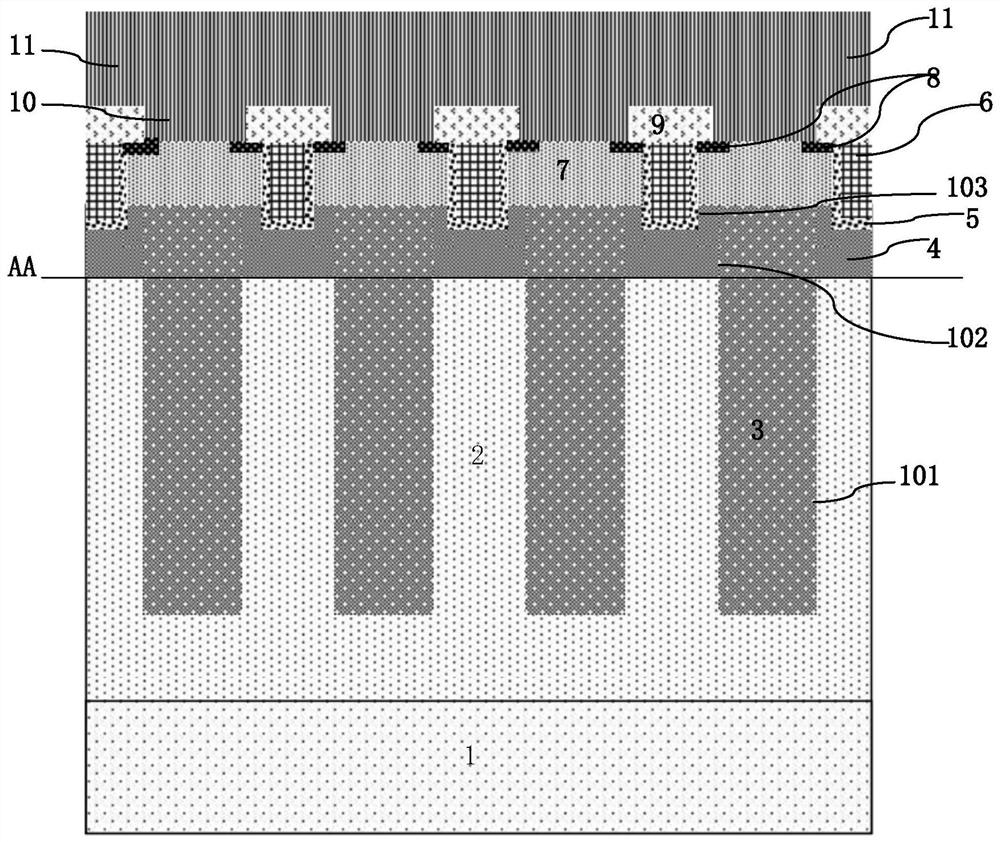
Figure 1 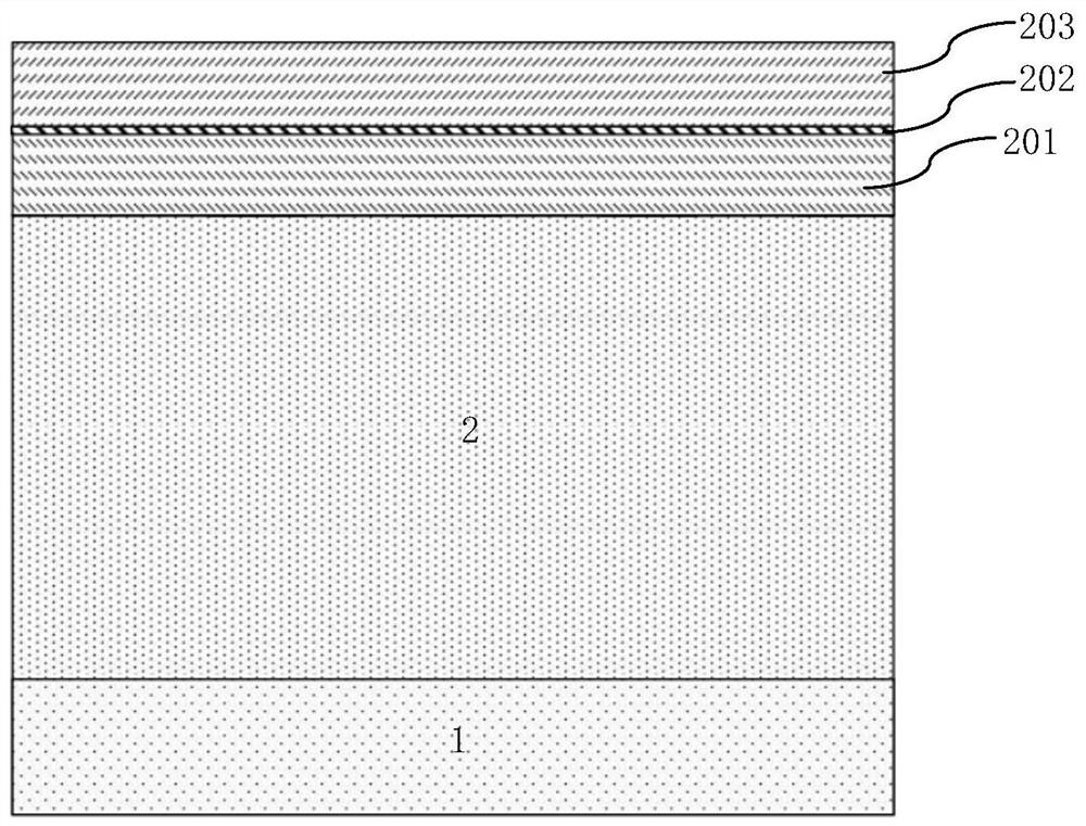
Figure 2 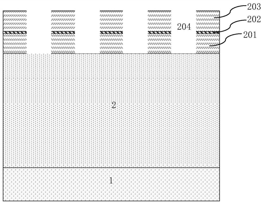
Figure 3
Abstract
Description
technical field
[0001] The invention relates to the field of semiconductor integrated circuit manufacturing, in particular to a trench gate super junction device; the invention also relates to a manufacturing method of the trench gate super junction device. Background technique
[0002] The superjunction is composed of alternately arranged P-type thin layers, also called P-type pillars (Pillar) and N-type thin layers, also called N-type pillars, formed in a semiconductor substrate, and the matching is completed by using P-type thin layers and N-type thin layers The formed depletion layer improves the reverse withstand voltage while maintaining a small on-resistance.
[0003] The super junction is usually formed by trench etching and trench epitaxial filling. First, a super junction trench is formed on the surface of the N-type epitaxial layer, and then a P-type epitaxial layer is filled in the super junction trench to form a P-type thin layer; N-type epitaxial layers betwee...
Examples
Embodiment Construction
[0051] Such as figure 1As shown, it is a schematic structural diagram of a trench-gate super-junction device according to an embodiment of the present invention; the trench-gate super-junction device according to an embodiment of the present invention includes:
[0052] The super junction trench 101 is formed in the first N-type epitaxial layer 2; a hard mask layer is formed on the surface of the first N-type epitaxial layer 2, and the super junction trench 101 is formed by the hard mask The first opening 204 is defined by layer photolithography. For the first opening 204 please refer to Figure 2B shown.
[0053] The P-type epitaxial layer 3 is filled in the super junction trench 101 and the first opening 204 at the top to form a P-type thin layer 3 .
[0054] After the P-type thin layer 3 is formed, the hard mask layer is removed and the P-type protrusion structure of the P-type thin layer 3 is formed, and the P-type protrusion structure is filled in the first opening 204...