
An amplitude and phase control chip and a bus type data transmission module
An amplitude-phase control, chip technology, applied in the direction of automatic power control, electrical digital data processing, electrical components, etc., can solve the problems of wasting line resources, increasing the number of channels, increasing the number of data lines, etc., to reduce the number of wiring, easy to high The effect of integration
Patent Information
- Authority / Receiving Office
- CN · China
- Current Assignee / Owner
- Publication Date
- 2019-01-08
Smart Images
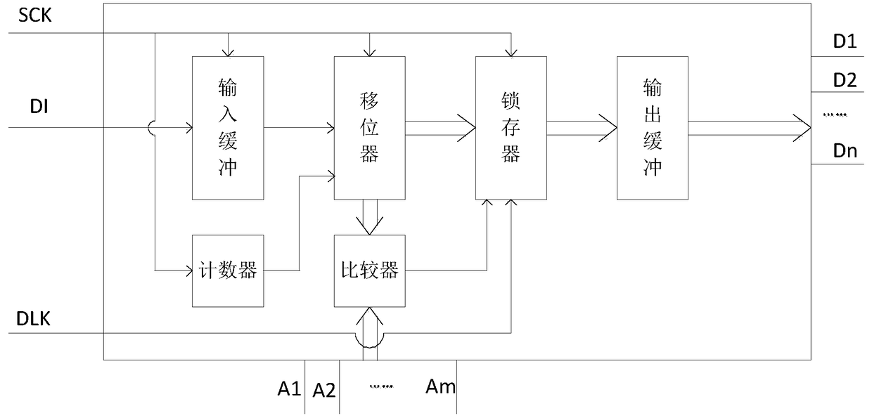
Figure 1 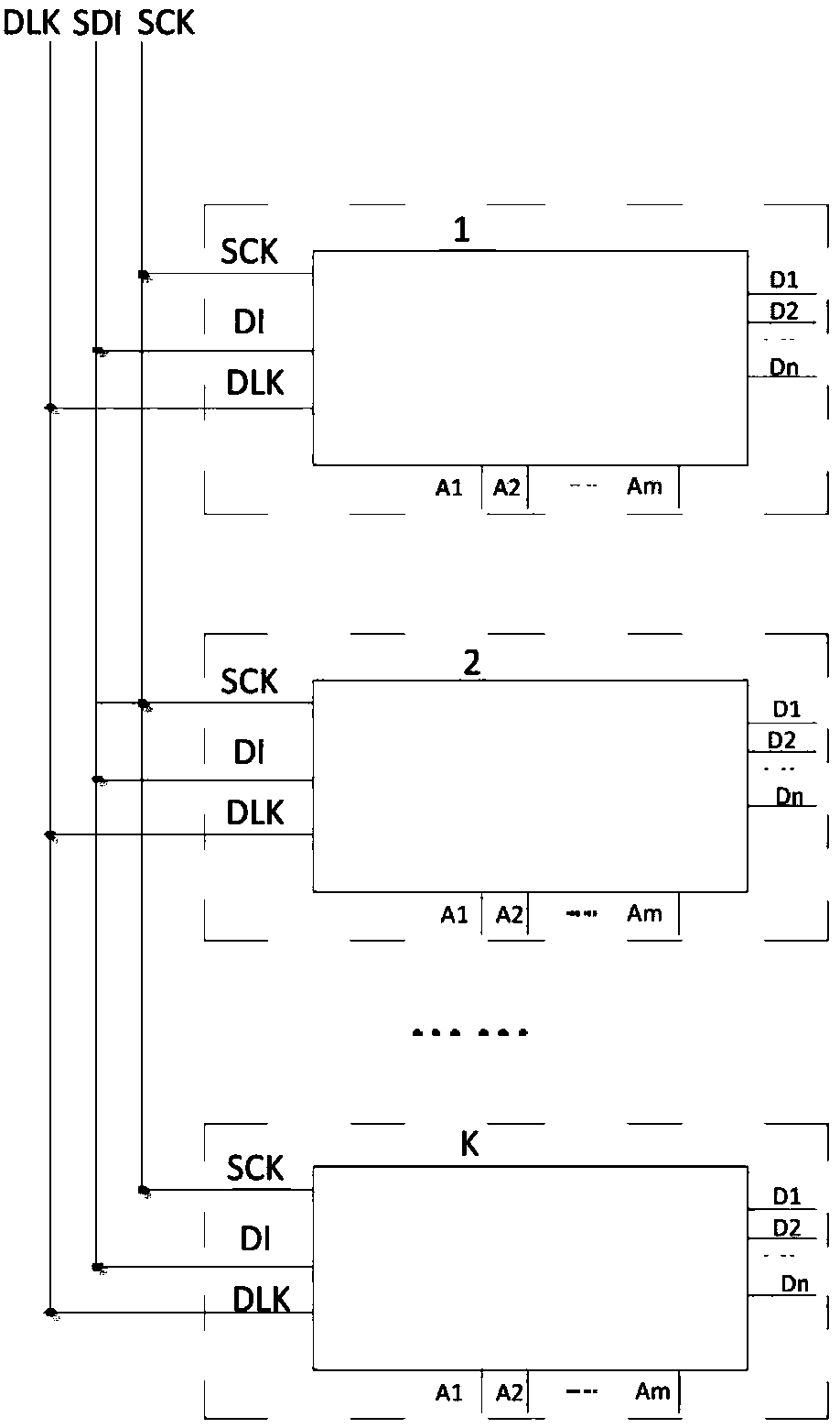
Figure 2 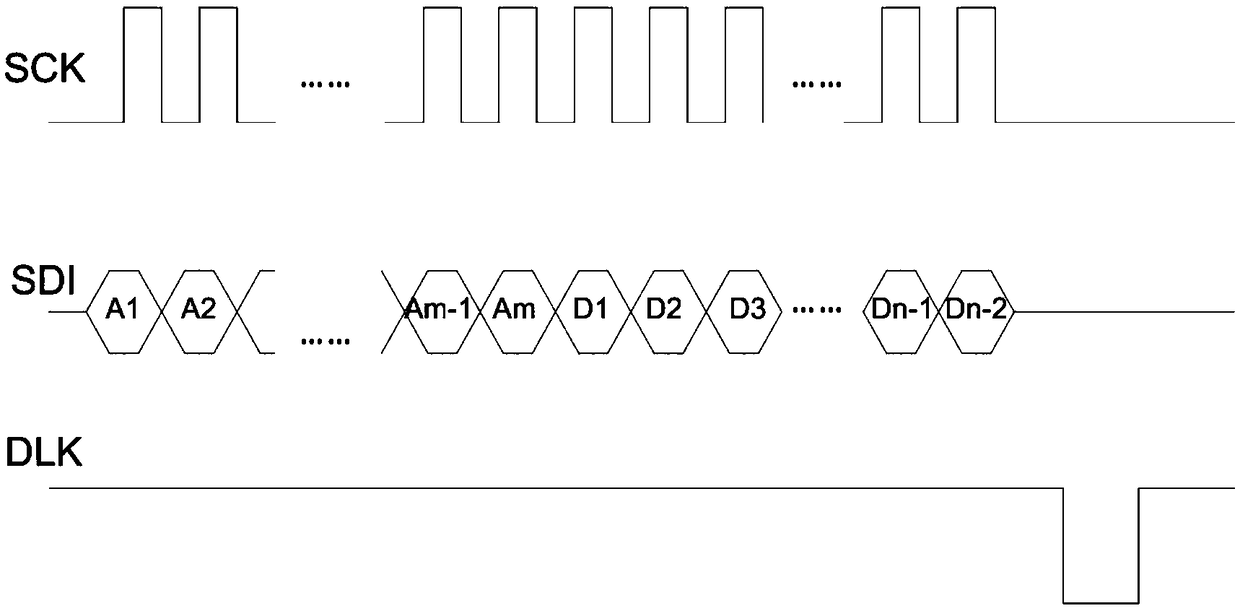
Figure 3
Abstract
Description
technical field
[0001] This application relates to the field of radar signal transmission, in particular to an amplitude and phase control chip and a bus-type data transmission component. Background technique
[0002] Compared with mechanical scanning radar, one of the most prominent features of phased array radar is that the antenna beam of phased array radar has agility capability, and the beam agility capability needs to be realized by real-time control of the amplitude and phase chips of each channel of the transceiver component. Traditional transceiver components use SPI (serial communication) communication, including data lines (SDI), clock lines (SCK), and latch lines (DLK). For multi-channel components, each channel needs a data line to achieve Amplitude and phase control for each channel. With the continuous improvement of volume and weight requirements of phased array radar, it is an inevitable trend to realize the development of highly integrated transceiver chan...
Examples
Embodiment 1
[0028] Such as figure 1 As shown, this example provides an amplitude and phase control chip, which encodes and sets the chip through the coding pins led out of the encoder, so that the chip is more convenient and uniformly defined in integrated use; the input data is internally checked by a comparator Matching identification is carried out to avoid the problem of data misinformation during integrated use. Specifically, the chip includes: a data input terminal, a shifter, a comparator, a latch and a data output terminal; the chip uses the data input terminal to input the data transmitted in the SPI bus to the shifter in the chip; The shifter compares the address bits in the input data, and if they match, the shifter transfers the data bits in the input data to the latch for latching, and the latched data is output through the data output terminal.
[0029] In this solution, since the data transmitted in the SPI bus includes address bits and data bits, in order to judge whether...
Embodiment 2
[0036] This example provides a data transmission scheme for phased array transceiver components, which can solve the problem of inconvenient wiring caused by the increasing number of transceiver component channels and the corresponding increase in data lines.
[0037] Such as figure 1 Shown is a schematic diagram of an amplitude and phase control chip. The chip includes: a clock signal input terminal SCK, a data input terminal DI, a latch signal input terminal DLK, an encoder with m codes (A1, ..., Am code bits), a data output terminal (D1, D2, ... , Dn); Obtain the clock signal, input data, and latch signal from the SPI bus through the above-mentioned input terminal, and encode the chip using the encoding pin drawn from the encoder. The chip also includes: input buffer block, shifter, latch, output buffer block, counter and comparator.
[0038] Such as figure 2 Shown is a schematic diagram of the bus data transmission components. The component includes: a plurality of K ...