
Novel ingot casting crucible sticking film and preparation method thereof
A crucible and ingot casting technology is applied in the field of new ingot casting crucible film and its preparation to achieve the effects of high conversion efficiency, improving purity and reducing impurities
Patent Information
- Authority / Receiving Office
- CN · China
- Patent Type
- Applications(China)
- Current Assignee / Owner
- Publication Date
- 2019-06-21
Smart Images
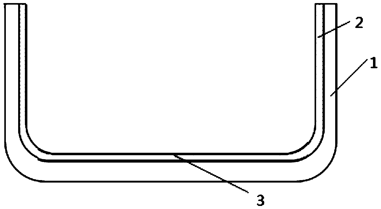
Figure 1 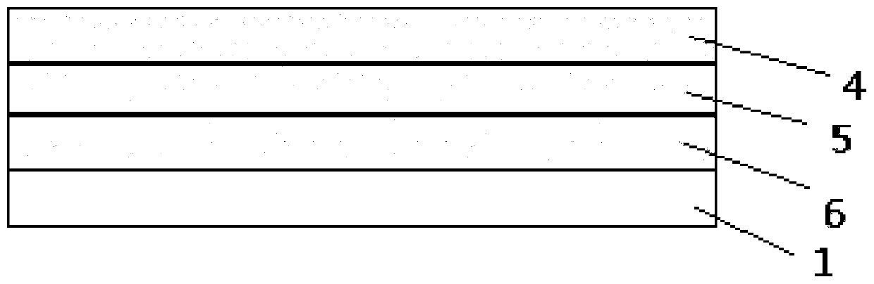
Figure 2 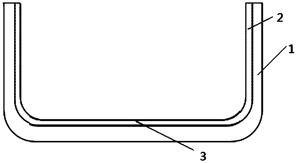
Figure 3
Abstract
Description
Technical field
[0001] The invention belongs to the technical field of preparation of silicon wafers for crystalline silicon solar cells, and relates to a novel ingot crucible film for improving the yield of crystalline silicon ingots and a preparation method thereof, in particular to a novel ingot crucible film and a preparation method thereof. Background technique
[0002] At present, crystalline silicon solar cells occupy a dominant position in the photovoltaic industry. The cost of silicon wafers accounts for more than half of the cost of crystalline silicon solar cells. Therefore, reducing the cost of silicon wafers and improving the quality of silicon wafers are extremely important for the development of the solar energy industry. Reduce the internal defects of silicon wafers, improve the quality of crystalline silicon wafers, and increase the yield of ingots as a direction for technical improvement.
[0003] In the crystalline silicon of traditional polycrystalline silicon ...
Examples
Embodiment 1
[0025] Electrophoresis deposition of the upper layer of silicon dioxide film containing Al powder
[0026] The specific solution components are ultrapure water, silica sol, high-purity silica, and Al powder. The slurry is prepared as follows: After weighting ultrapure water, silica sol, high-purity silica (purity of 99.999%, particle diameter of 10μm-20μm), and Al powder in a weight ratio of 100:1:5:0.1, First, put the ultrapure water, silica sol, and Al powder into a mixer and mix them evenly for 30 minutes to form a stable suspension, then mix with high-purity silicon dioxide particles and mix them evenly for 30 minutes and then stand for use.
[0027] When performing electrophoretic deposition of thin films, the process parameters are as follows: working voltage is 10-20V, working current is 4-5A, solution temperature is 80°C, and time is 30min.
[0028] The made crucible film, the upper layer of the film is The film thickness of the uniformly aligned silica particles is 100μm, ...
Embodiment 2
[0036] Electrophoresis deposition of upper layer of silicon dioxide film containing Ni powder
[0037] The specific solution components are ultrapure water, silica sol, silica powder, and Ni powder. The preparation of the slurry is as follows: the ultrapure water, silica sol, silicon powder (particle diameter of 10μm-20μm), Ni powder in a weight ratio of 100:1:5:0.1 after the weight, the ultrapure water, silica sol , Ni powder is put into a mixer and stirred evenly for 30 minutes to form a stable suspension, then mixed with silicon powder (particle diameter is 10μm-20μm) and stirred evenly for 30 minutes and then stand for use.
[0038] When performing electrophoretic deposition of thin films, the process parameters are as follows: working voltage is 10-20V, working current is 4-5A, solution temperature is 80°C, and time is 30min.
[0039] The prepared crucible film has a silicon powder particle film thickness of 100 μm on the film, a carbon fiber structure film in the middle layer ...
Embodiment 3
[0047] Electrophoresis deposition of upper silicon dioxide film
[0048] The specific solution components are ultrapure water, silica sol, and high-purity silica. The slurry is prepared as follows: the ultrapure water, silica sol, high-purity silicon dioxide (purity of 99.999%, particle diameter of 10μm-20μm) in a weight ratio of 100:1:5, then the ultrapure water , The silica sol is put into a mixer and stirred evenly for 30 minutes to form a stable suspension, then mixed with high-purity silicon dioxide particles and stirred evenly for 30 minutes, and then set aside.
[0049] When performing electrophoretic deposition of thin films, the process parameters are as follows: working voltage is 10-20V, working current is 4-5A, solution temperature is 80°C, and time is 30min.
[0050] The prepared crucible film, the upper layer of the film is dense silica particles with a thickness of 100 μm, the middle layer of the film is a carbon fiber structure film with a thickness of 1 mm, and the ...