
Complicated Curved Thin Film Transistor and Self-Aligned Electric Fluid Conformal Photolithography Fabrication Method
A thin-film transistor, complex curved surface technology, applied in semiconductor/solid-state device manufacturing, circuits, electrical components, etc., to improve safety and stability, improve resolution, and avoid erosion
Patent Information
- Authority / Receiving Office
- CN · China
- Patent Type
- Patents(China)
- Current Assignee / Owner
- Publication Date
- 2022-03-18
Smart Images
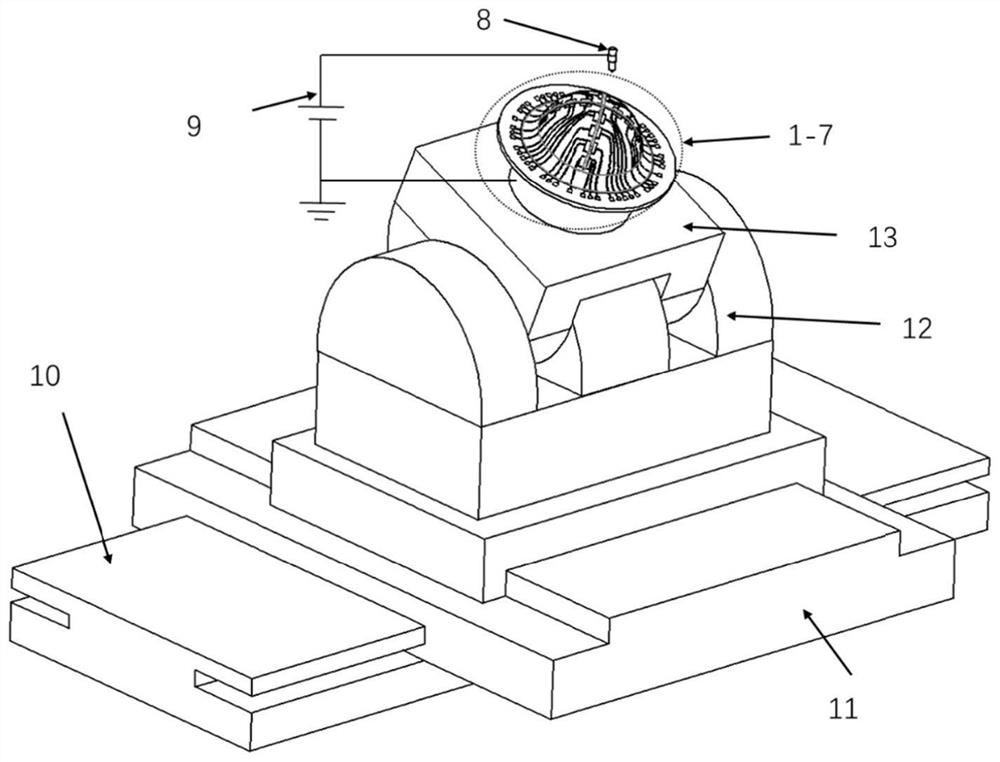
Figure 1 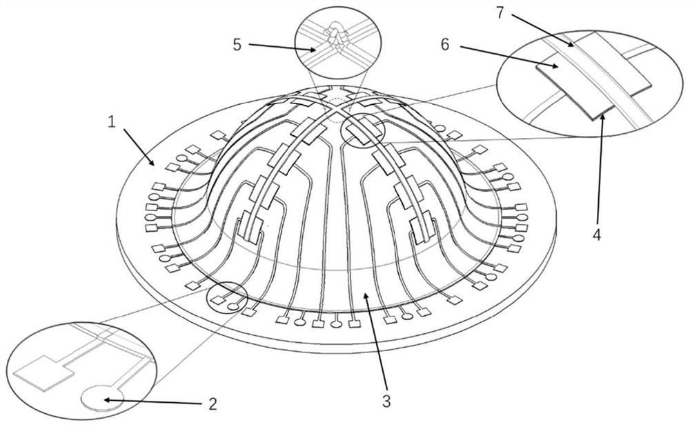
Figure 2 
Figure 3
Abstract
Description
technical field
[0001] The invention belongs to the technical field related to the preparation of organic thin film transistors, and more specifically, relates to a complex curved surface thin film transistor and a self-aligned electrofluid conformal lithography manufacturing method, in particular to an organic thin film with small channels on a complex curved surface substrate Transistor Self-Aligned Electrofluidic Conformal Lithographic Fabrication Method. Background technique
[0002] Organic thin-film transistor (OTFT) is the key driving electronic component of the next-generation display technology and multi-functional sensor in the future. The channel length (L) of its key feature structure has micro-nano dimensions. The current preparation process relies heavily on traditional lithography technology. Traditional lithography technology relies heavily on the manufacturing accuracy of the mask, the chemical properties of the photoresist, and the wavelength of the light s...
Examples
Embodiment Construction
[0036] In order to make the object, technical solution and advantages of the present invention clearer, the present invention will be further described in detail below in conjunction with the accompanying drawings and embodiments. It should be understood that the specific embodiments described here are only used to explain the present invention, not to limit the present invention. In addition, the technical features involved in the various embodiments of the present invention described below can be combined with each other as long as they do not constitute a conflict with each other.
[0037] see figure 1 , figure 2 , Figure 4 and Figure 5 , the present invention provides a self-aligned electrofluid conformal lithography manufacturing method of complex curved surface thin film transistors, the preparation method is a self-aligned electrofluid conformal lithography manufacturing method, which includes the following steps:
[0038]Step 1, preparing a three-dimensional cur...