
Silicon carbide split gate mosfet cell with integrated gated diode and preparation method
A gated diode and silicon carbide technology, which is applied in the manufacture of diodes, electrical components, semiconductor/solid-state devices, etc., can solve the problems of high conduction voltage drop of SiC body diode, high density of JFET area, and increase of dynamic loss of devices. Improved long-term reliability, reduced on-voltage, and reduced Miller capacitance
Patent Information
- Authority / Receiving Office
- CN · China
- Patent Type
- Patents(China)
- Current Assignee / Owner
- Publication Date
- 2022-07-12
Smart Images
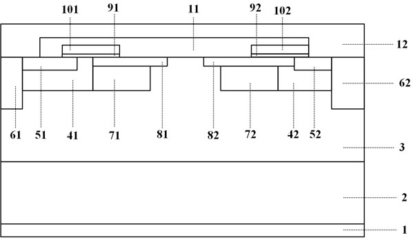
Figure 1 
Figure 2 
Figure 3
Abstract
Description
technical field
[0001] The invention belongs to the technical field of power semiconductor devices, and in particular relates to a silicon carbide separated gate MOSFET cell with integrated gate-controlled diode and a preparation method thereof. Background technique
[0002] The wide-bandgap semiconductor material SiC is an ideal material for the preparation of high-voltage power electronic devices. Compared with Si material, SiC material has a high breakdown electric field strength (4×10 6 V / cm), high carrier saturation drift velocity (2×10 7 cm / s), high thermal conductivity, good thermal stability, etc., so it is especially suitable for high-power, high-voltage, high-temperature and radiation-resistant electronic devices.
[0003] SiC VDMOS is a commonly used device in SiC power devices. Compared with bipolar devices, since SiCVDMOS has no charge storage effect, it has better frequency characteristics and lower switching losses. At the same time, the wide band gap of SiC...
Examples
Embodiment Construction
[0045] The principles and features of the present invention will be described below with reference to the accompanying drawings. The examples are only used to explain the present invention, but not to limit the scope of the present invention.
[0046] This embodiment provides a silicon carbide split gate MOSFET cell with integrated gated diode, such as figure 1 As shown, it includes a backside ohmic contact alloy 1, an N-type doped silicon carbide substrate 2, an N-type doped silicon carbide epitaxial layer 3, a first P-type doped well region 41, a second P-type doped well region 42, The first N-type doped source region 51, the second N-type doped source region 52, the first P-type doped source region 61, the second P-type doped source region 62, the first P-type doped buried layer 71, The second P-type doped buried layer 72, the first N-type doped guide layer 81, the second N-type doped guide layer 82, the first gate oxide layer 91, the second gate oxide layer 92, the first p...