
Liquid crystal display device and driving method to be used in same
Patent Information
- Authority / Receiving Office
- US · United States
- Current Assignee / Owner
- Publication Date
- 2005-04-21
- Estimated Expiration
- Not applicable · inactive patent
Smart Images
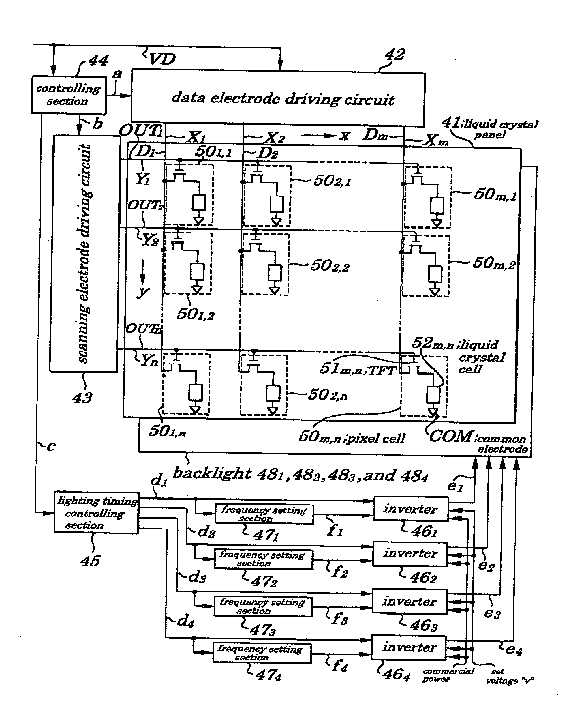
Figure 1 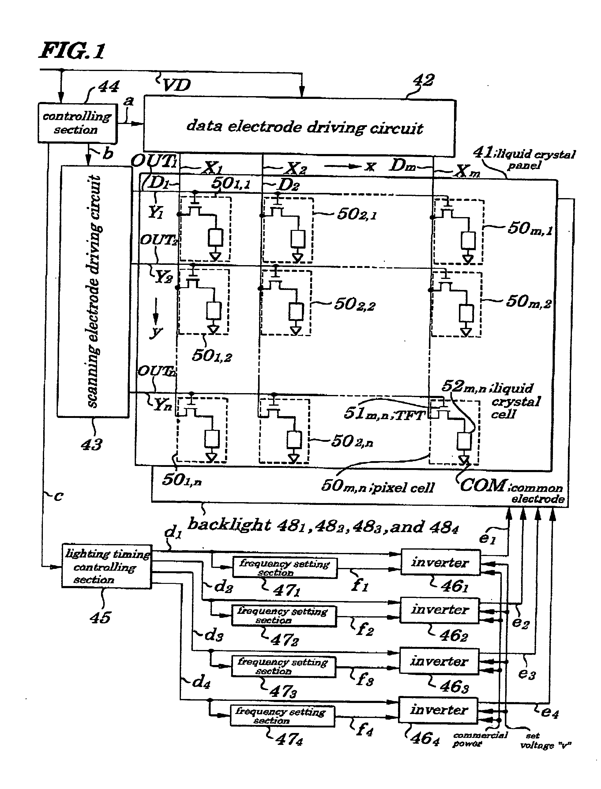
Figure 2 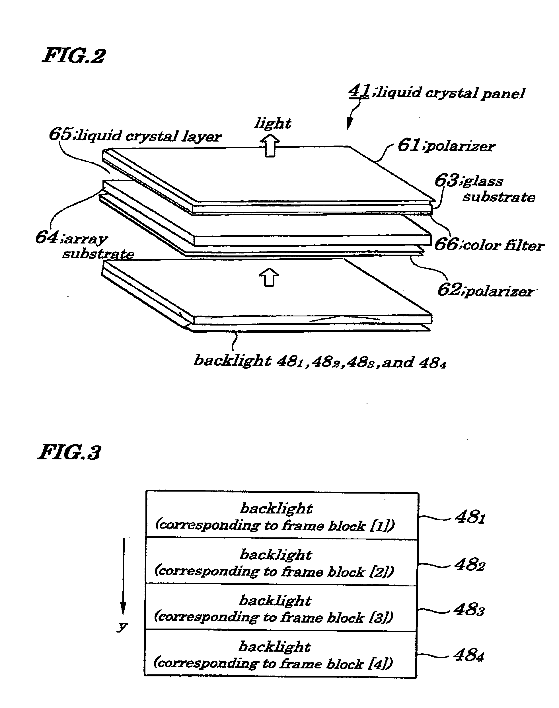
Figure 3
Abstract
Description
BACKGROUND OF THE INVENTION
[0001] 1. Field of the Invention
[0002] The present invention relates to a liquid crystal display device and a driving method to be used in the liquid crystal display device and more particularly to the liquid crystal display device having a surface light source, such as a cold cathode fluorescent tube, which lights up when a driving pulse voltage is applied to from an inverter and the driving method to be used in the above liquid crystal display device.
[0003] The present application claims priority of Japanese Patent Application No. 2003-358591 filed on Oct. 17, 2003, which is hereby incorporated by reference.
[0004] 2. Description of the Related Art
[0005] In recent years, among image display devices, a liquid crystal display device, in particular, is made larger in size and high-definition and is used not only in a device to display freeze-frame images in such a personal computer and / or word processor but also in a device to display moving images such...
Examples
first embodiment
[0109]FIG. 1 is a schematic block diagram showing electrical configurations of a liquid crystal display device of a first embodiment of the present invention. The liquid crystal display of the first embodiment, as shown in FIG. 1, includes a liquid crystal panel 41, a data electrode driving circuit 42, a scanning electrode driving circuit 43, a controlling section 44, a lighting timing controlling section 45, inverters 461, 462, 463, and 464, and frequency setting sections 471, 472, 473, and 474, and backlights 481, 482, 483, and 484. The liquid crystal panel 41 is made up of data electrodes Xi (i=1, 2, . . . , m; for example, m=640×3), scanning electrodes Yj (j=1, 2, . . . , n; for example, n=512), and pixel cells 50i, ,j (i=1, 2, . . . , m; j=1, 2, . . . , n). The data electrodes Xi are arranged at specified intervals in an “x” direction, to which a voltage corresponding to pixel data Di (i=1, 2, . . . , m) is applied. The scanning electrodes Yj are arranged at specified intervals...
second embodiment
[0123]FIG. 6 is a schematic block diagram showing electrical configurations of a liquid crystal display device according to a second embodiment of the present invention. In FIG. 6, same reference numbers are assigned to components corresponding to those employed in the first embodiment shown in FIG. 1. The liquid crystal display device of the second embodiment includes a light timing controlling section 45A and frequency setting section 47A instead of the lighting timing controlling section 45 and frequency setting sections 471, 472, 473, and 474 shown in FIG. 1, wherein functions of the light timing controlling section 45A and the frequency setting section 47A are different from those of the lighting timing controlling section 45 and the frequency setting sections 471, 472, 473, and 474 shown in FIG. 1, and additionally includes a voltage setting section 49. The inverters 462, 463, and 464 (inverter 461 is retained) are not mounted and, instead of the backlights 481, 482, 483, and ...
third embodiment
[0129]FIG. 9 is a schematic block diagram showing electrical configurations of a liquid crystal display device according to a third embodiment of the present invention. In FIG. 9, same reference numbers are assigned to components corresponding to those in the first and second embodiments shown in FIGS. 1 and 6. The liquid crystal display device of the third embodiment, as shown in FIG. 9, includes, in addition to components used in the liquid crystal display device shown in FIG. 1, voltage setting sections 491, 492, 493, and 494 each having the same function as the voltage setting section 49 shown in FIG. 6. The voltage setting sections 491, 492, 493, and 494 do setting of voltages v1, v2, v3, and v4 to be applied to inverters 461, 462, 463, and 464 so that each of driving pulse voltages “e1”, “e2”, “e3”, and “e4” gradually increases from its initial value to a set value during a period from start time of lighting of each of backlights 481, 482, 483, and 484 to a specified time. Oth...