
Circuit device
Patent Information
- Authority / Receiving Office
- US · United States
- Current Assignee / Owner
- Publication Date
- 2005-10-13
- Estimated Expiration
- Not applicable · inactive patent
Smart Images
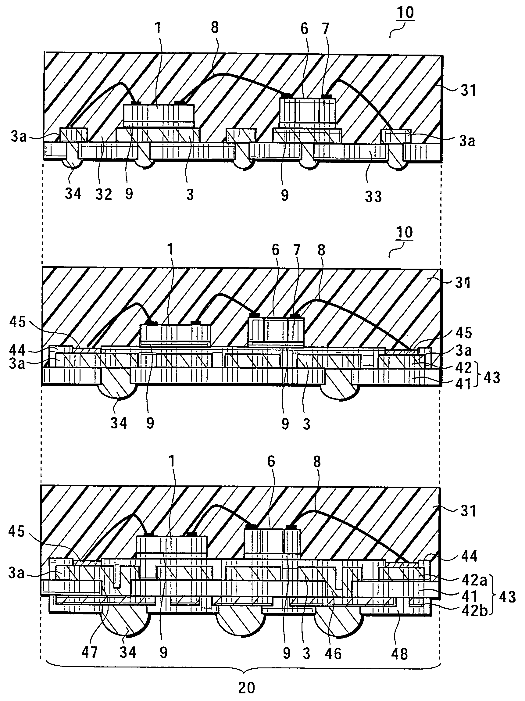
Figure 1 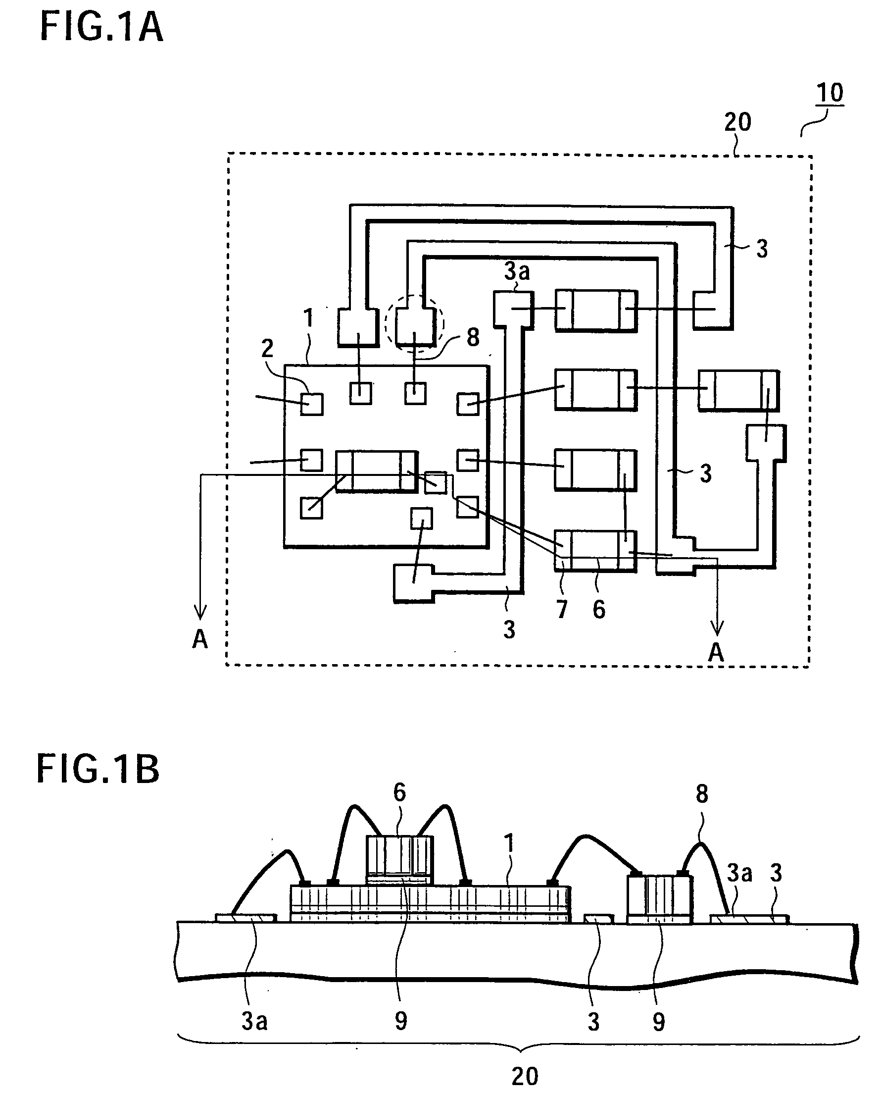
Figure 2 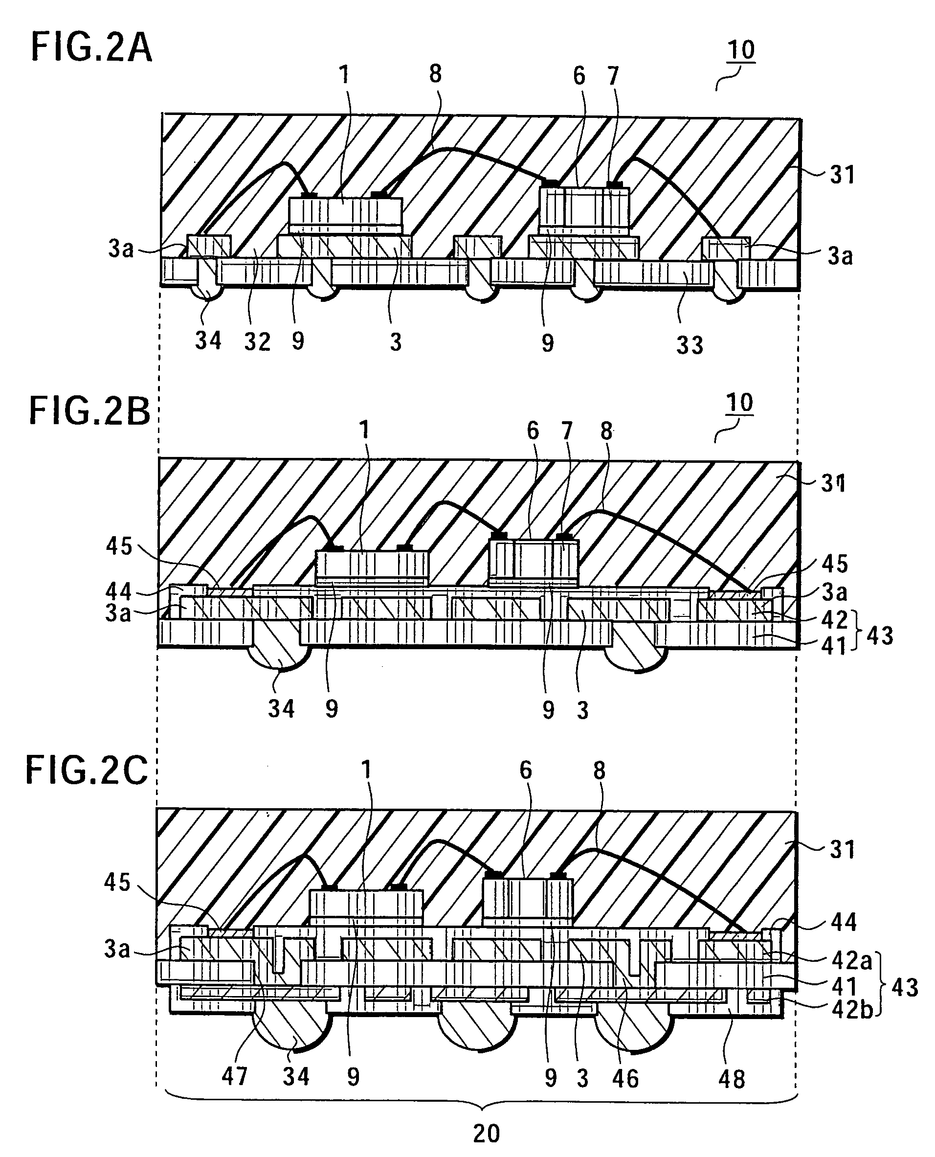
Figure 3
Abstract
Description
BACKGROUND OF THE INVENTION
[0001] 1. Field of the Invention
[0002] The present invention relates to a circuit device including a passive element, and more particularly relates to a circuit device having an improved wiring density.
[0003] 2. Description of the Related Art
[0004] With reference to FIGS. 5A and 5B, a conventional circuit device will be described. FIG. 5A is a plan view of the circuit device, and FIG. 5B is a cross-sectional view along the line B-B in FIG. 5A.
[0005] As shown in FIG. 5A, a semiconductor element 101 such as an IC, for example, and a plurality of conductive patterns 103 are arranged in a predetermined package region 120 on a supporting substrate 110, for example. The conductive patterns 103 include a pad part 103a to which a bonding wire 108 or the like is fixed, and / or mounting land parts 103b to which both electrode parts 107 of a passive element 106 are fixed. The passive element 100 is, for example, a chip condenser or the like.
[0006] The passive el...
Examples
Embodiment Construction
[0035] With reference to FIGS. 1 to 4, an embodiment of a circuit device according to an embodiment of the present invention will be described.
[0036]FIGS. 1A and 1B show the circuit device of this embodiment. FIG. 1A is a plan view, and FIG. 1B is a cross-sectional view along the line A-A in FIG. 1A.
[0037] The circuit device 10 of this embodiment includes a semiconductor element 1, conductive patterns 3, passive elements 6, and bonding wires 8.
[0038] As shown in FIG. 1A, the circuit device has a package region 20 in a predetermined region indicated by the broken line, for example. Note that, in the package region 20 of this embodiment, at least the semiconductor element 1 such as an IC, for example, the conductive patterns 3, and the passive elements 6 are disposed. Here, the package region 20 is one continuous region indicated by the dotted line forming a predetermined circuit. The conductive pattern 3 has a pad part 3a on its end, to which the bonding wire 8 is fixed.
[0039] In...