
Test pads for IC chip
a technology of ic chips and test pads, which is applied in the direction of individual semiconductor device testing, semiconductor/solid-state device testing/measurement, instruments, etc., can solve the problems of difficult placement of test probes and layout differences, and achieve the effect of saving chip area
Patent Information
- Authority / Receiving Office
- US · United States
- Patent Type
- Applications(United States)
- Current Assignee / Owner
- Publication Date
- 2006-02-09
- Estimated Expiration
- Not applicable · inactive patent
Smart Images
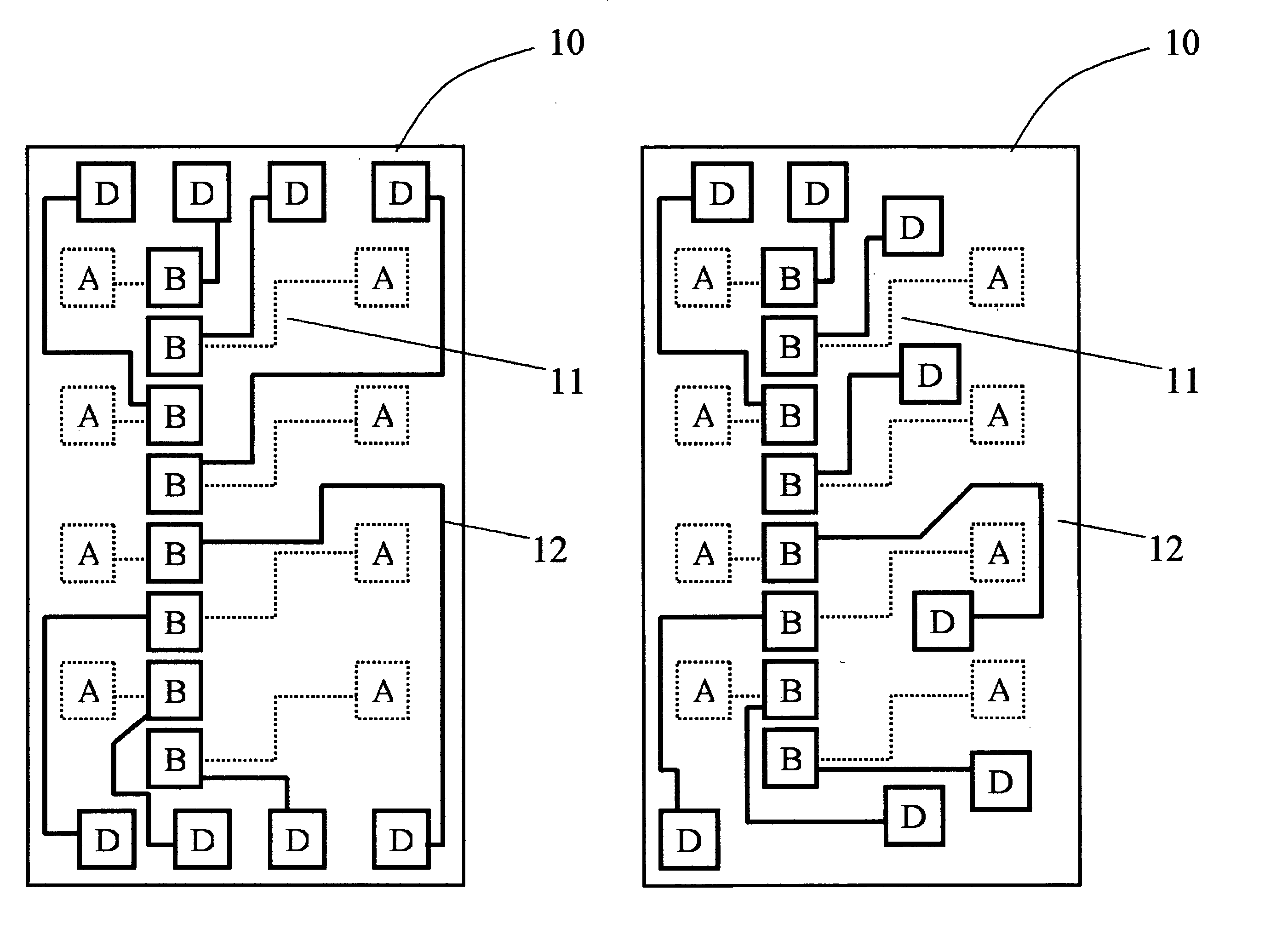
Figure 1 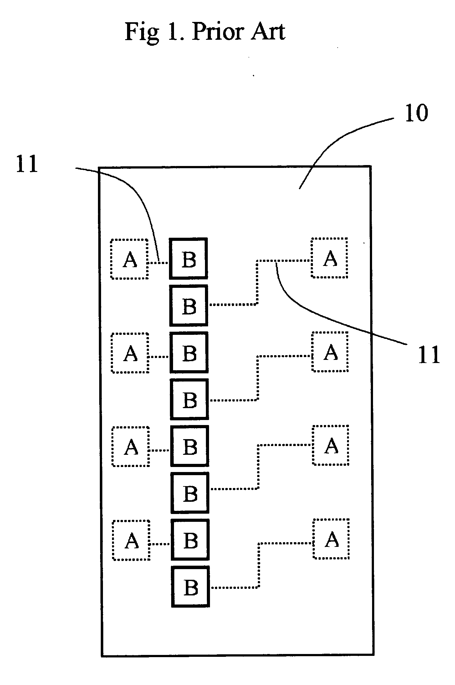
Figure 2 
Figure 3
Abstract
Description
BACKGROUND OF THE INVENTION
[0001] 1. Field of the Invention
[0002] The invention relates to layout of bonding pads of an IC chip, particularly to the layout of the bonding pads for testing the chip
[0003] 2. Brief Description of Related Art
[0004] In testing an IC chip, the test pads on the chip must be spaced far enough to allow the test probes to access. In recent development, there has been an approach to package more than one chip together. In such a case, the test pads require additional consideration. Recent development of the “board on chip” also requires the pads be arranged along a straight line in the middle of the chip.
[0005] FIG. 1 shows a prior art test pads layout. An IC chip 10 includes bonding pads “A” placed along the edges of the chip. To facilitate the interconnection with an adjacent chip (not shown), the bonding pads are rearranged and aligned along a straight line as pads “B” to shorten wire-bonding.
[0006] As an illustration, the chip 10 has eight metal bondi...
Examples
Embodiment Construction
[0014] The basic layout of the present invention is shown in FIG. 3. In the prior art chip 10 shown in FIG. 1, additional test pads “D” are added along the two ends of the chip 10. The test pads are alternately connected to the closely-spaced group “B” pads. The spacing between the group “D” pads are wider than the spacing between the group “B” pads to allow the group “D” pads accessible to test probes. The connections between the group “B” pads and the group “D” pads are separate from and not in series with the connections between the group “A” pads and the group “B” pads.
[0015]FIG. 4 shows a second embodiment of the present invention, where the test pads D are arranged in open area of the chip.
[0016] While the preferred embodiment of the invention has been described, it will be apparent to those skilled in the art that various modifications may be made without departing from the spirit of the invention. Such modifications are all within the scope of the present invention.