
Integrated circuit clock grid drive optimization method based on drive windows
A technology of clock grid and integrated circuit, applied in electrical digital data processing, special data processing applications, instruments, etc., can solve problems such as poor layout, difficult timing convergence, wiring congestion, etc., to save chip area occupation, good reliability The effect of scalability
Patent Information
- Authority / Receiving Office
- CN · China
- Current Assignee / Owner
- Publication Date
- 2014-03-05
Smart Images
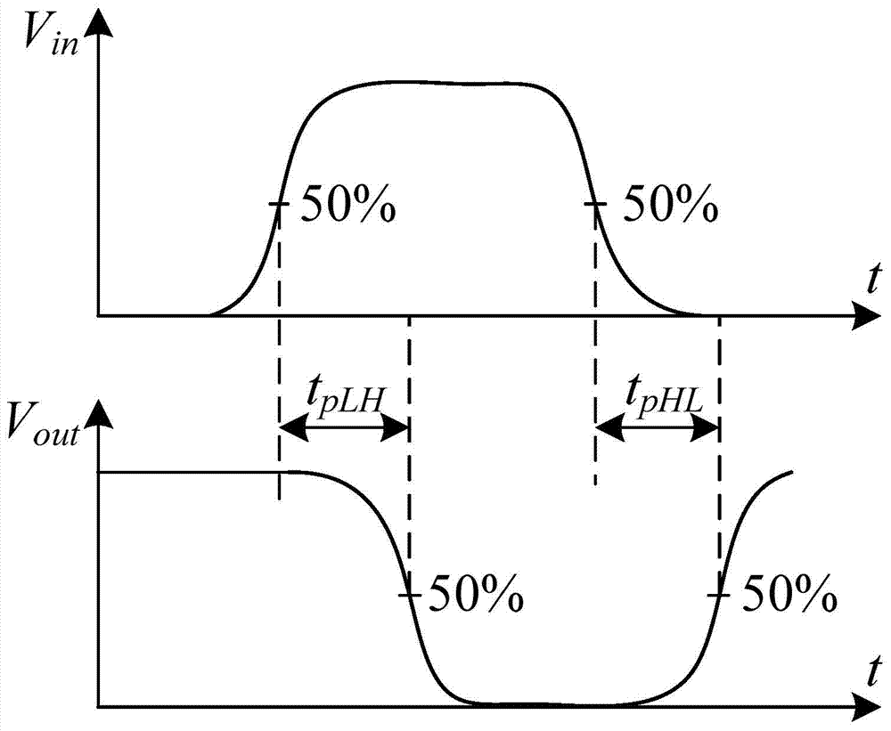
Figure 1 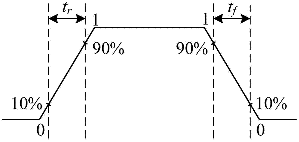
Figure 2 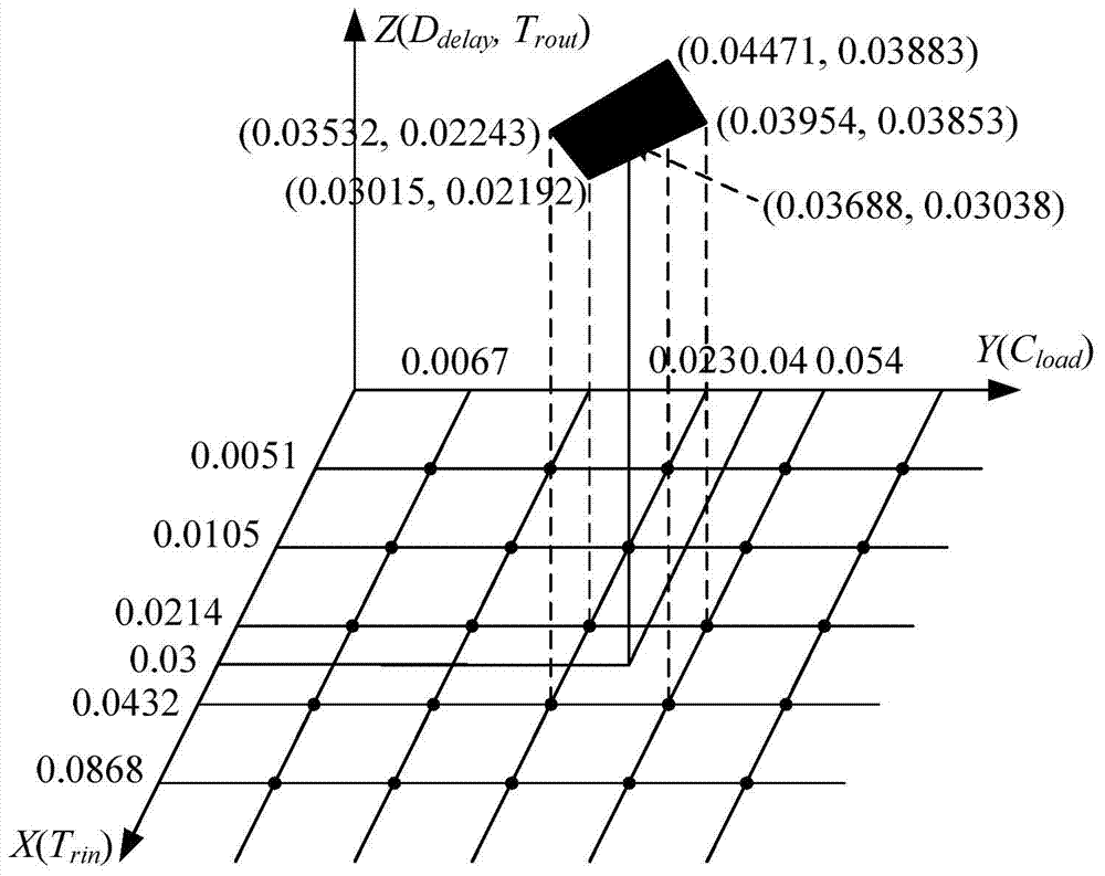
Figure 3
Abstract
Description
technical field
[0001] The present invention relates to the field of integrated circuit (Integrated Circuit, hereinafter referred to as IC) design automation field of microelectronics technology, in particular to an integrated circuit clock grid driving optimization method based on a driving window. Background technique
[0002] In the physical design of semi-custom integrated circuits, devices are basically selected from the cell library provided by the process manufacturer, so the timing and physical indicators of the cells need to be specially considered to meet various design requirements. The timing of the device mainly refers to the device delay and the output signal transition time, and the physical index of the device mainly concerns the size of the unit area.
[0003] The device delay indicates the time elapsed when a signal passes through a logic gate. Generally, the time required for a 50% change in the input signal voltage to a 50% change in the output signal vol...
Examples
Embodiment Construction
[0023] like Figure 4 As shown, the implementation steps of the integrated circuit clock grid driving optimization method based on the driving window in this embodiment are as follows:
[0024] 1) Based on the low-pass filtering characteristics, the clock grid of the integrated circuit is divided into multiple driver windows according to the influence range of each driver, and one driver window is taken as the current driver window, and then jump to step 2).
[0025] In this embodiment, the driving window obtained by dividing the clock grid of the integrated circuit into a rectangular window, each main intersection point of the clock grid is located at the center of the rectangular window, specifically as follows Figure 5 As shown, the triangles in the figure represent the drivers placed at the intersections of the grid backbones, and each rectangular area represents the influence range of the corresponding driver—the driving window, and the small black dots in it represent t...