

Plasma etching method
a technology of etching method and substrate material, which is applied in the direction of fluid pressure measurement, instruments, vacuum gauges, etc., can solve the problems of etching size error, complex task, and inability to accurately etch substrate material, so as to achieve accurate etching effect and execute
Patent Information
- Authority / Receiving Office
- US · United States
- Current Assignee / Owner
- Publication Date
- 2006-02-23
- Estimated Expiration
- Not applicable · inactive patent
Smart Images
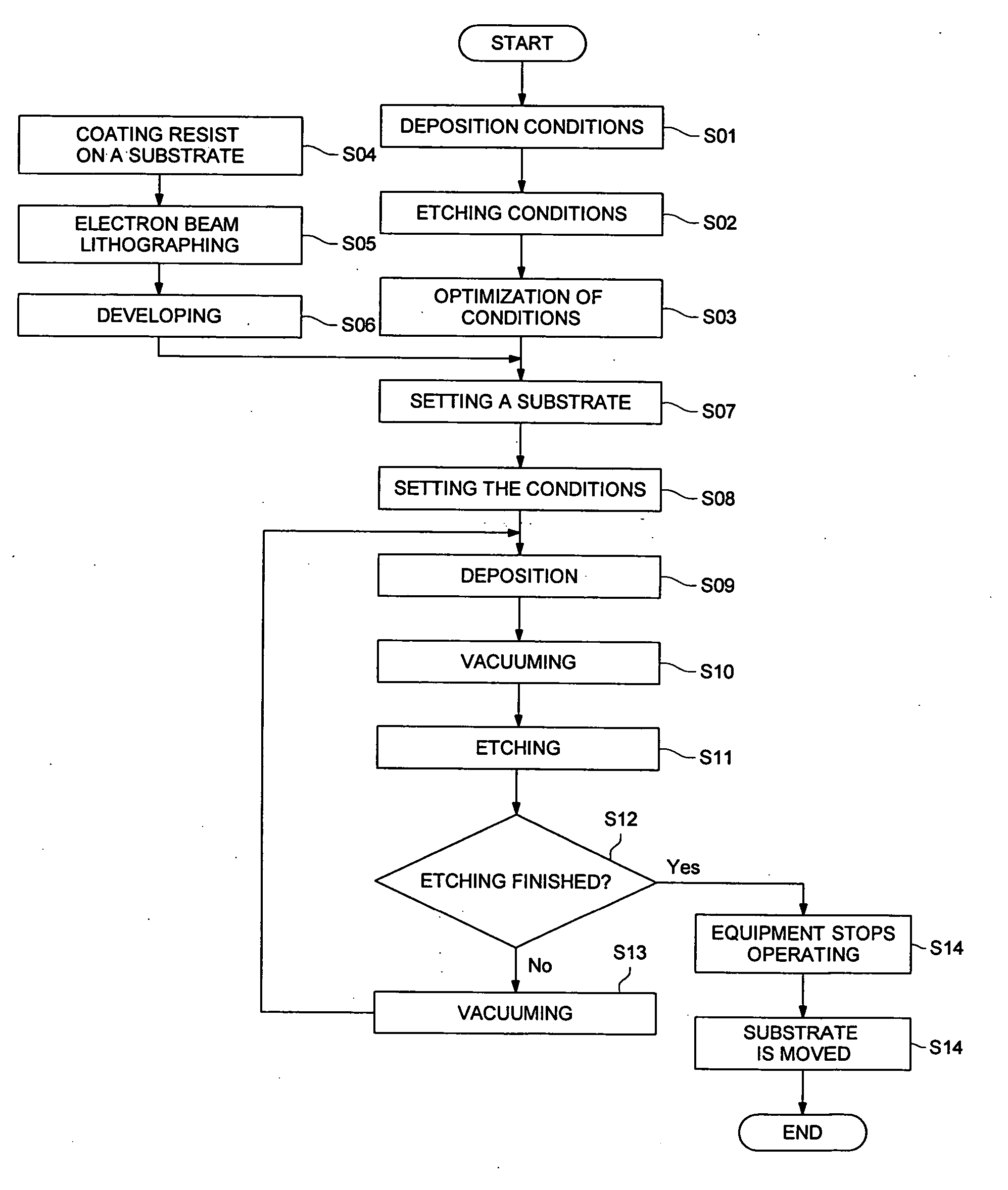
Figure 1 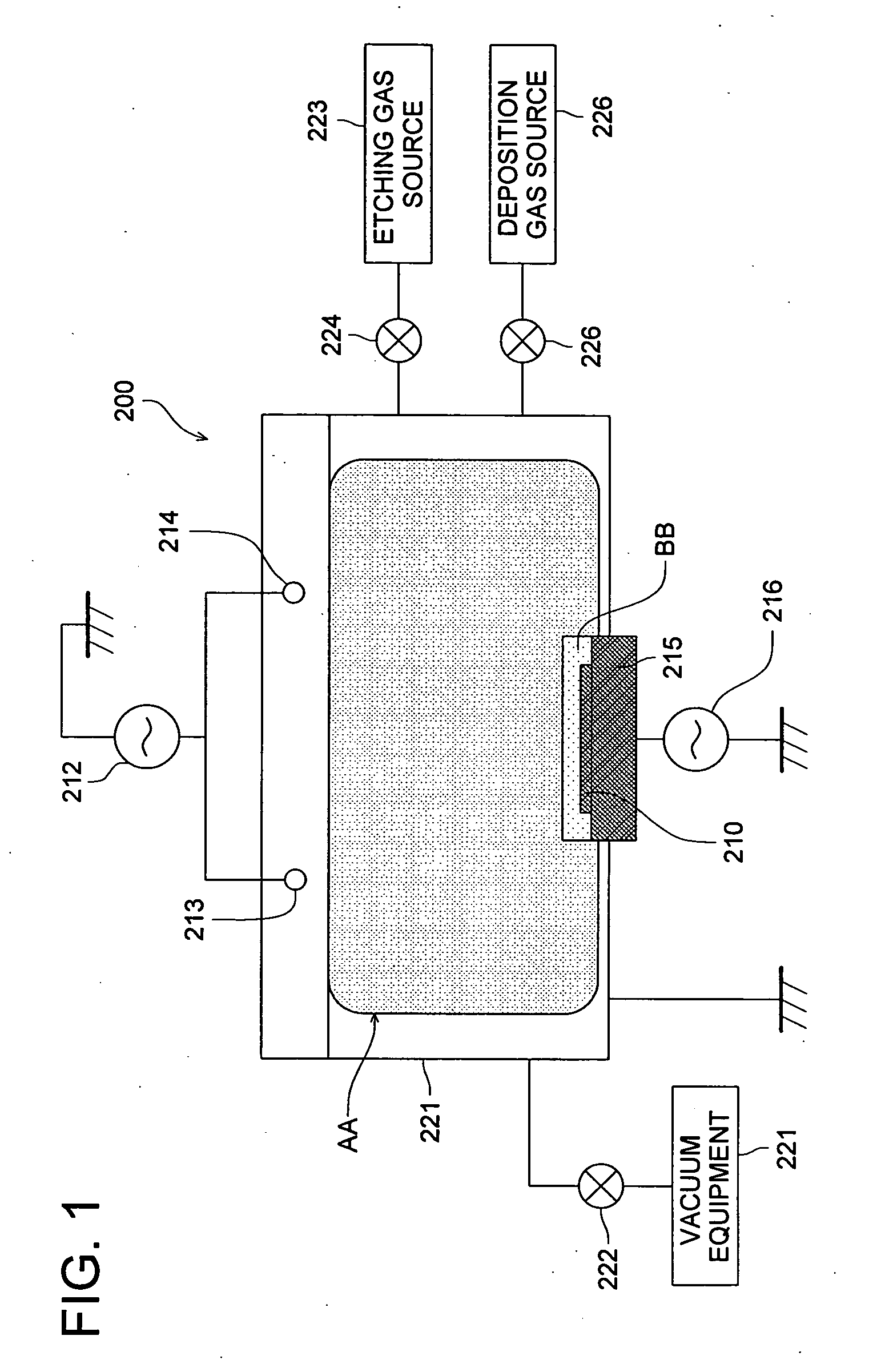
Figure 2 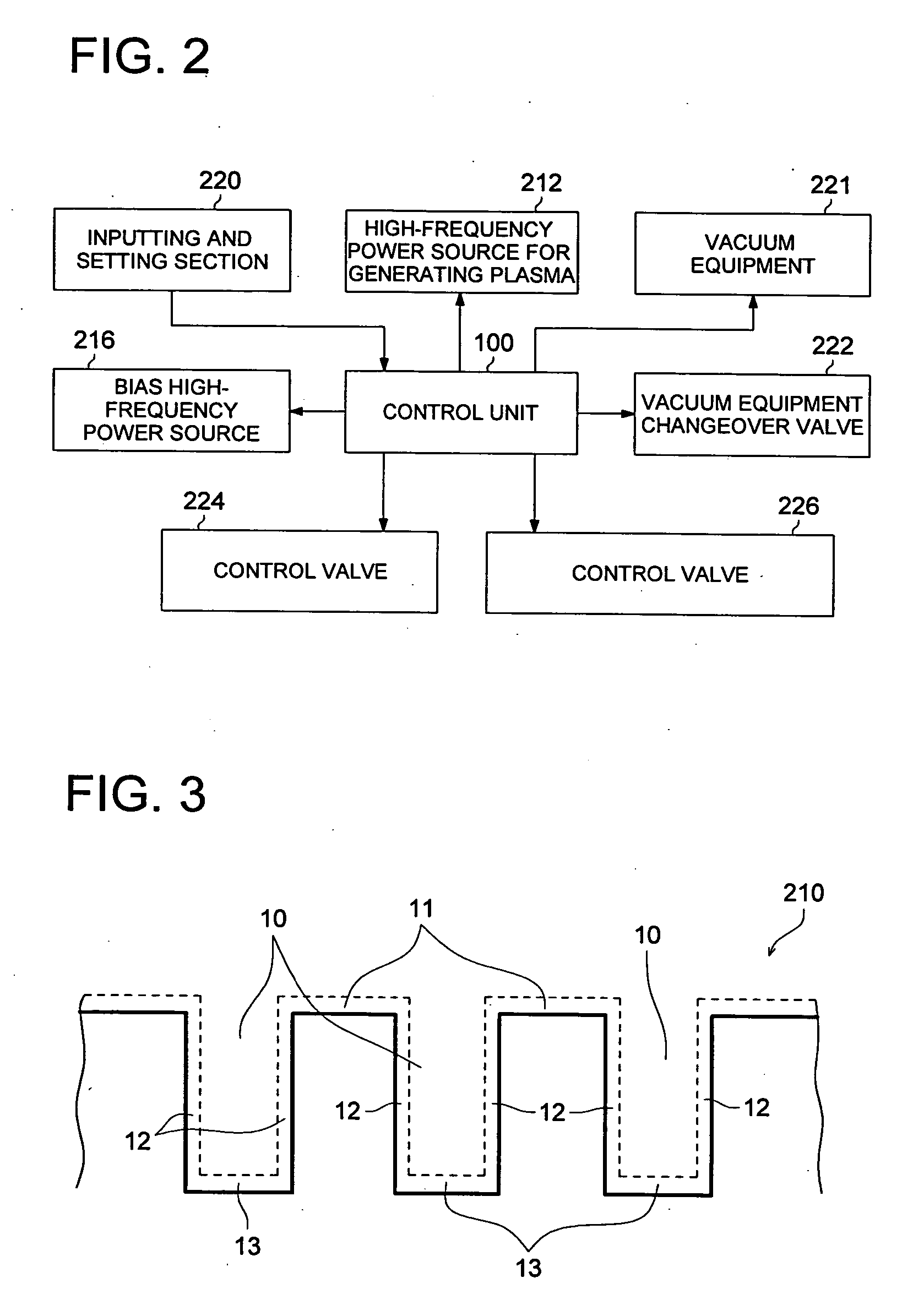
Figure 3
Abstract
Description
BACKGROUND OF THE INVENTION
[0001] 1. Field of the Invention
[0002] The present invention relates to a plasma etching method that uses plasma to process a substrate material such as silicon.
[0003] 2. Description of the Related Art
[0004] Conventionally, a plasma etching method, which is a dry etching technique, has been used to etch substrates made of silicon or the like. To increase performance of semiconductor elements or to manufacture dies for large-scale integrated elements, more complicated and highly accurate substrate etching techniques have been required. Specifically, the plasma etching method has been widely applied to silicon because of silicon's excellent etching characteristics. The plasma etching is a method in which by introducing reactive gas into the vacuum (in, for example, vacuum chamber) and applying a high-frequency electric field, accelerated electrons collide with gas molecules thereby converting the gas into plasma that consists of positive ions, electrons,...
Examples
embodiment
[0099] Next, the plasma etching method according to the present invention will be specifically described through embodiments 1 through 4.
[0100] In embodiment 1, a recessed and protruding pattern is created on a silicon substrate at the 200-nm cycle. In embodiment 2, a recessed and protruding pattern is created on a silicon substrate at the 600-nm cycle. In embodiment 3, a four-story step-like pattern is created on a silicon substrate. In embodiment 4, a saw-edged pattern is created on a silicon substrate.
[0101] The name of the ICP etching system and process conditions used in embodiments 1 through 4 are as described below, and the deposition process and the etching process were repeatedly and alternately conducted with the vacuuming process (vacuuming) interposed between the two processes according to the timing shown in FIG. 10.
embodiments 1 and 2
[0102] Equipment maker: ULVAC, Inc., model: CE300I, equipment name: ICP etching system [0103] Gas (1) (deposition gas): C4F8 [0104] Deposition gas pressure: 1.33 Pa [0105] Gas (2) (etching gas): SF6 / O2 [0106] Etching gas pressure: 0.3 Pa [0107] Plasma excitation high-frequency output during deposition: 300 W [0108] Plasma excitation high-frequency output during etching: 150 W [0109] Bias output: 3 W [0110] Vacuum pressure during vacuuming process: 0.006-0.009 Pa
embodiments 3 and 4
[0111] Equipment maker: ULVAC, Inc., model: CE300I, equipment name: ICP etching system [0112] Gas (1) (deposition gas): C4F8 [0113] Deposition gas pressure: 1.33 Pa [0114] Gas (2) (etching gas): SF6 / O2 [0115] Etching gas pressure: 0.6 Pa [0116] Plasma excitation high-frequency output during deposition: 300 W [0117] Plasma excitation high-frequency output during etching: 120 W [0118] Bias output: 5 W [0119] Vacuum pressure during vacuuming process: 0.006-0.009 Pa
[0120]FIG. 11 shows scanning type electron micrographs of a recessed and protruding pattern (200-nm period) created on the resist etching mask formed on the surface of the silicon substrate in the embodiment 1 and the etched recessed and protruding pattern. FIG. 11(a) shows the recessed and protruding pattern created on the etching mask, and FIG. 11(b) shows an etched recessed and protruding pattern. The recessed and protruding pattern shape of the etching mask is period 200 nm, space 90 nm wide, line 110 nm wide, 280 nm hig...