
Semiconductor device and method for manufacturing the same
a semiconductor device and semiconductor technology, applied in the field of light emitting, can solve problems such as acceleration of deterioration of light emitting devices
Patent Information
- Authority / Receiving Office
- US · United States
- Patent Type
- Applications(United States)
- Current Assignee / Owner
- Publication Date
- 2006-08-24
- Estimated Expiration
- Not applicable · inactive patent
Smart Images
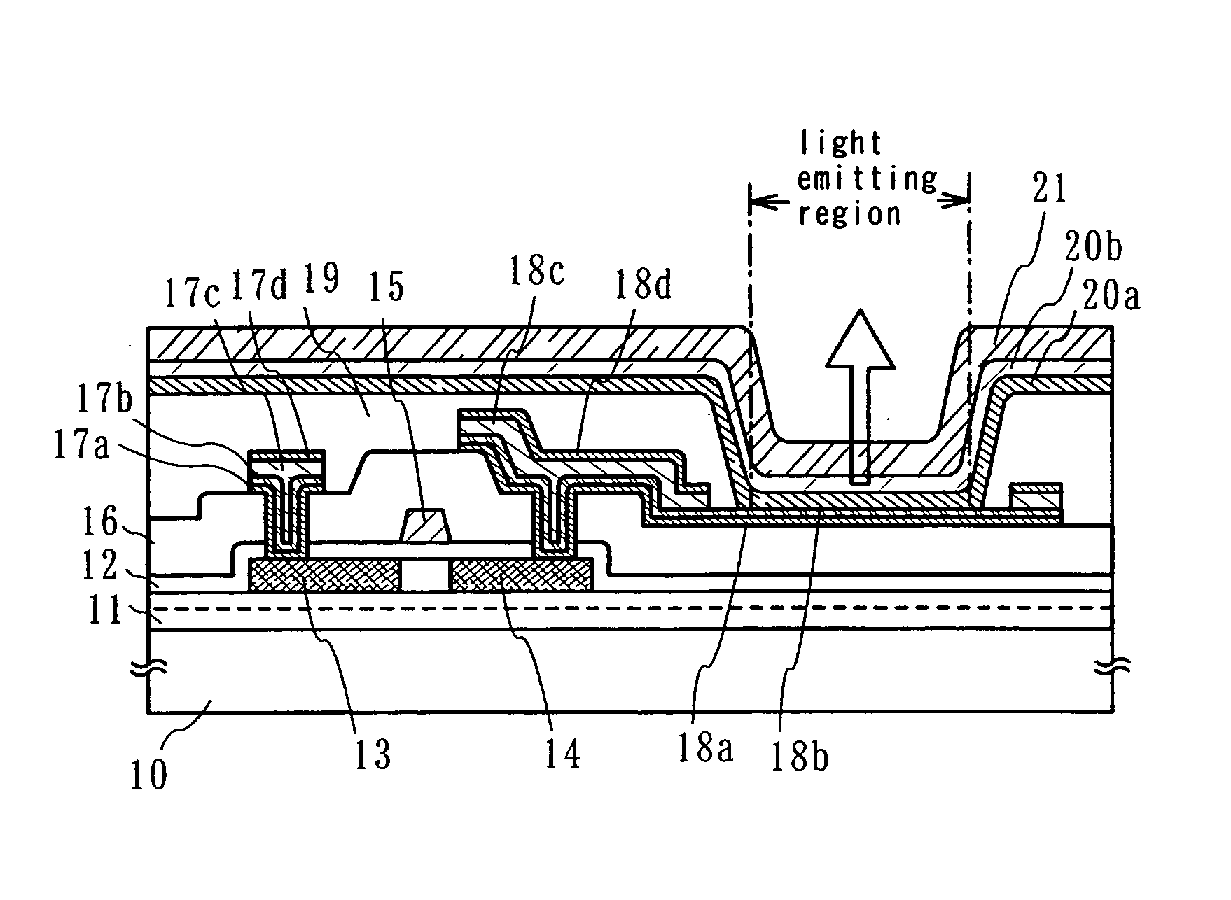
Figure 1 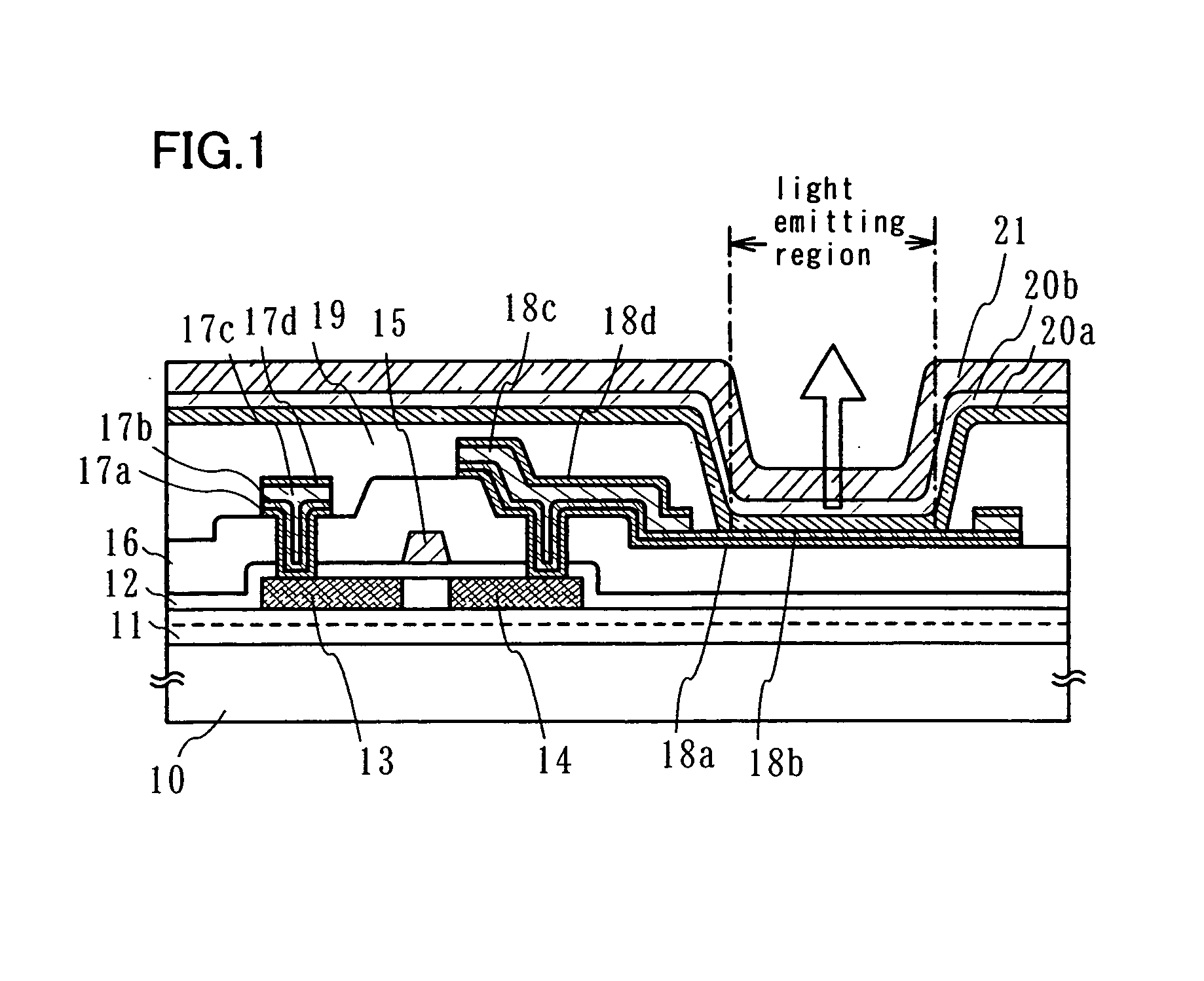
Figure 2 
Figure 3
Abstract
Description
BACKGROUND OF THE INVENTION
[0001] 1. Field of the Invention
[0002] The present invention relates to a light emitting device with a light emitting element that emits fluorescent light or phosphorescent light upon application of electric field to a pair of electrodes of the element which sandwich a layer containing an organic compound (hereinafter, an organic compound layer), and to a method of manufacturing the light emitting device. Further, the present invention relates to a deposition apparatus for forming an organic compound layer or the like.
[0003] 2. Description of the Related Art
[0004] Light emitting elements, which use organic compounds as a light emitting member and are characterized by the thinness, lightweight, fast response, and direct current low voltage driving, are expected to be applied to next-generation flat panel displays. Among display devices, ones having light emitting elements arranged in matrix are considered to be particularly superior to conventional liqu...
Examples
embodiment mode 1
[0063]FIG. 1 is a cross-sectional view of an active matrix light emitting apparatus (a part of one pixel).
[0064] In FIG. 1, a TFT (p-channel TFT) provided over a substrate 10 having an insulating surface controls current flowing to a second EL layer 20b which emits light of blue, red, or green. Reference numerals 13 and 14 denote a source region or a drain region. A glass substrate, a plastic substrate, or the like can be used as the substrate 10. Alternatively, a semiconductor substrate or a metal substrate which has an insulating film on the surface can be used. A base insulating film 11 is formed over the substrate 10 (here, a bottom layer is a nitride insulating film and a top layer is an oxide insulating film). A gate insulating film 12 is provided between a gate electrode 15 and a semiconductor layer. Reference numeral 16 denotes an interlayer insulating film formed of with a single layer or a stack of an inorganic material, such as silicon oxide, silicon nitride, silicon nit...
embodiment mode 2
[0097]FIG. 3 shows an example of a structure according to this embodiment mode which is different from the one in Embodiment Mode 1. FIG. 3 shows a structure in which a first electrode is not directly in contact with a semiconductor layer of a TFT, but is electrically connected to the semiconductor layer of the TFT through another electrode. The first electrode has a structure in which a first region formed with a single metal layer and a second region having three layers are provided, and a step is caused between the first region and the second region. In order to improve the aperture ratio, the first region is provided at only the periphery of the contact hole, and the second region is provided in all the other regions.
[0098] In this embodiment mode, an example of forming a pixel area and a driver circuit over one substrate will be described.
[0099] First, as in Embodiment Mode 1, a base insulating film 311, a semiconductor layer formed with a crystalline semiconductor film, and ...
embodiment mode 3
[0125] Here, several methods for manufacturing a full-color display device will be described. Specifically, a method in which three light emitting elements are used; a method in which a white light emitting element and a color filter are used in combination; a method in which a blue light emitting element and a color conversion layer are used in combination; a method in which a white light emitting element, a color conversion layer, and a color filter are used in combination; or the like may be used.
[0126] In the case of using three light emitting elements for performing full color display, pixels each of which is provided with a red light emitting element, a blue light emitting element, and a green light emitting element, which are regularly arranged are arranged in a pixel area. For example, three kinds of evaporation masks having different opening positions for each light emission colors of R, G, and B, thereby providing light emitting layers of R, G, and B by vapor deposition. ...