
Power-on solution to avoid crowbar current for multiple power supplies' inputs/outputs
Patent Information
- Authority / Receiving Office
- US · United States
- Current Assignee / Owner
- Publication Date
- 2006-10-05
Smart Images
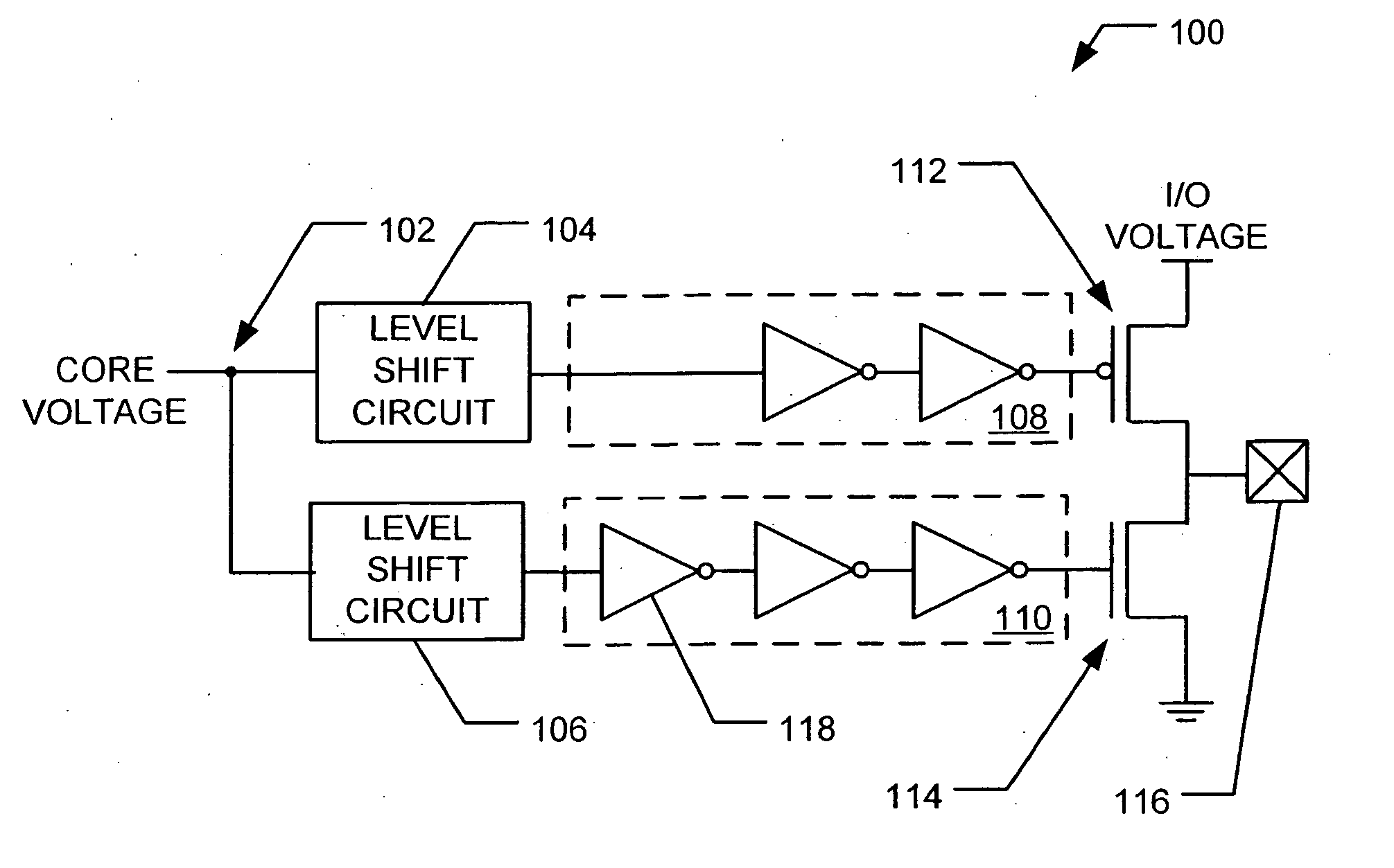
Figure 1 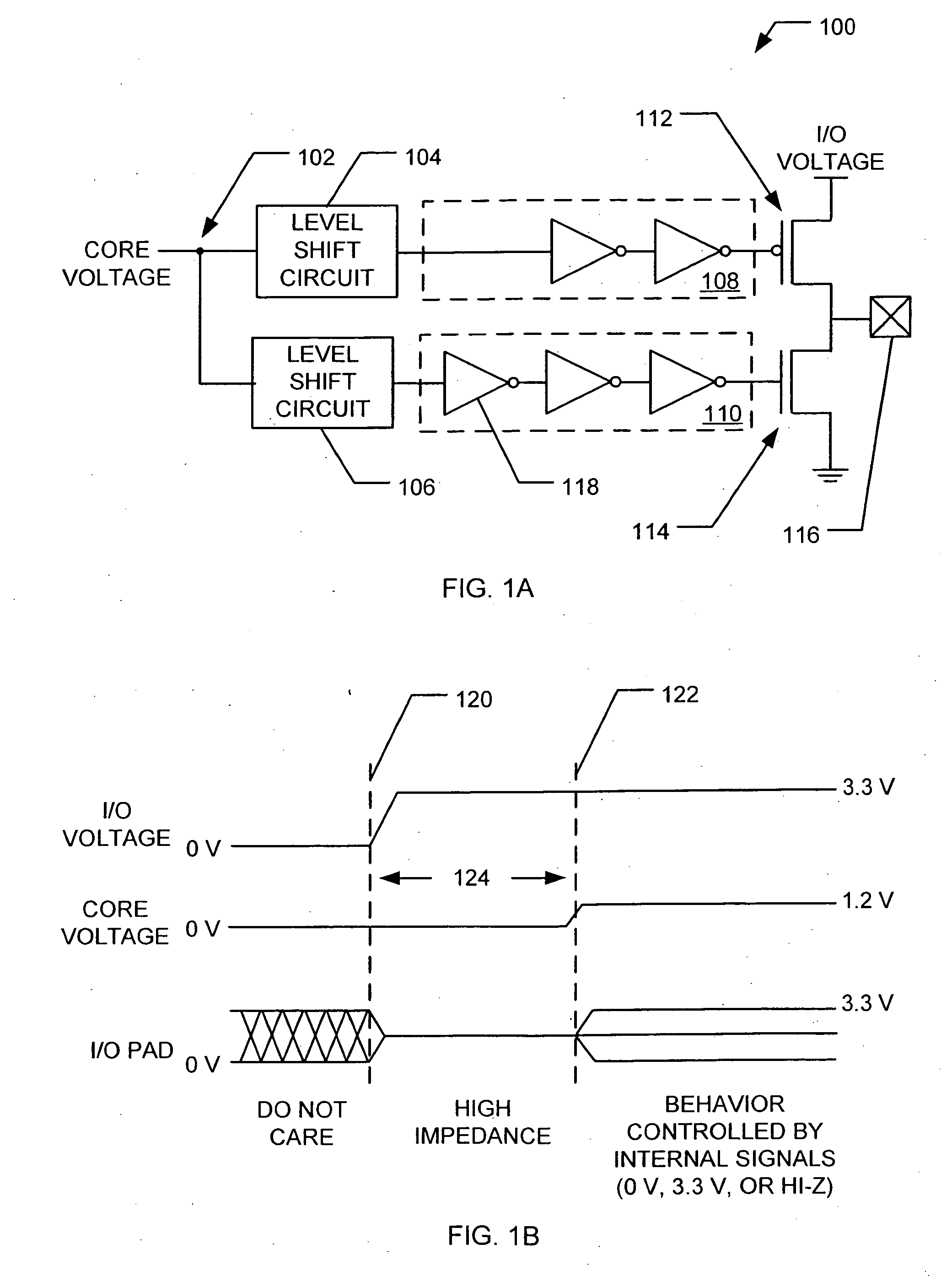
Figure 2 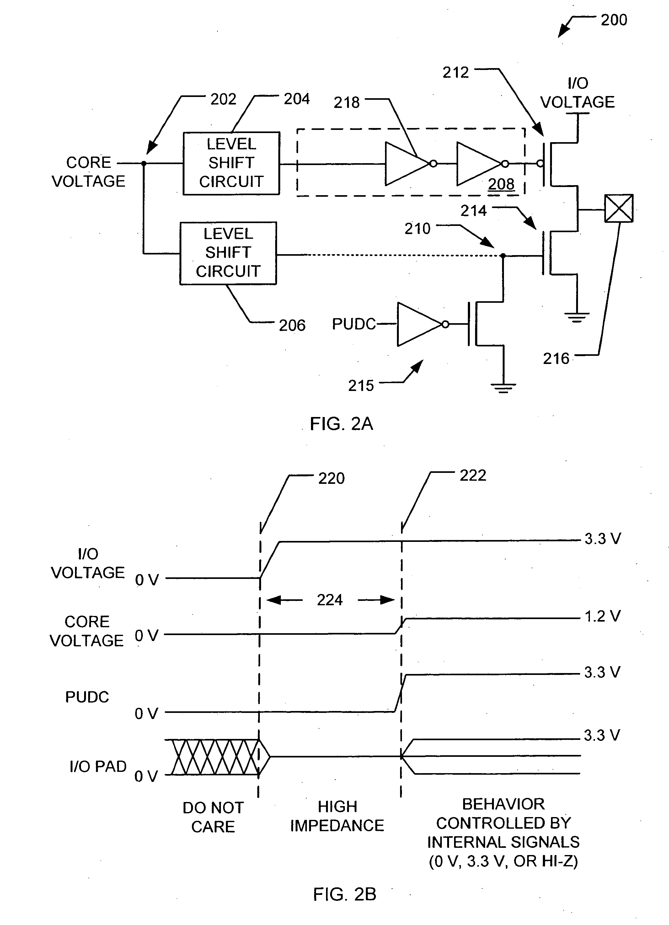
Figure 3
Abstract
Description
BACKGROUND OF THE INVENTION
[0001] The present invention is directed to integrated circuits and their processing for the manufacture of semiconductor devices. More particularly, the invention provides a method and device for avoiding crowbar current during power-on of integrated circuits. Merely by way of example, the invention has been applied to input / output (I / O) interfaces with multiple power supplies. But it would be recognized that the invention has a much broader range of applicability.
[0002] Integrated circuits have evolved from a handful of interconnected devices fabricated on a single chip of silicon to millions of devices. Conventional integrated circuits provide performance and complexity far beyond what was originally imagined. In order to achieve improvements in complexity and circuit density (i.e., the number of devices capable of being packed onto a given chip area), the size of the smallest device feature, also known as the device “geometry”, has become smaller wit...
Examples
Embodiment Construction
[0018] According to the present invention, techniques directed to integrated circuits are provided. More particularly, the invention provides a method and device for avoiding, or substantially reducing, crowbar current. Merely by way of example, the invention has been applied to I / O interfaces for integrated circuits with multiple power supplies. But it would be recognized that the invention has a much broader range of applicability.
[0019]FIG. 1A is a simplified schematic of an integrated circuit 100 according to an embodiment of the present invention. This diagram is merely an example, which should not unduly limit the scope of the claims. One of ordinary skill in the art would recognize many variations, alternatives, and modifications. Integrated circuit 100 includes a node 102 at a core voltage, or a first supply voltage level. Upon power-on, core voltage increases over a short period of time from 0 volts to a predetermined voltage. In one embodiment, the predetermined voltage i...