
Photoelectric converting film stack type solid-state image pickup device
a technology of photoelectric and solid-state image, which is applied in the direction of electrical equipment, semiconductor devices, radio frequency control devices, etc., can solve the problems of bad production yield, quantity of photoelectric charges accumulated, and ccd-type image sensors or cmos-type image sensors reaching the limit of their technical progress, so as to achieve efficient removal of photoelectric charges
Patent Information
- Authority / Receiving Office
- US · United States
- Patent Type
- Applications(United States)
- Current Assignee / Owner
- Publication Date
- 2008-06-12
- Estimated Expiration
- Not applicable · inactive patent
Smart Images
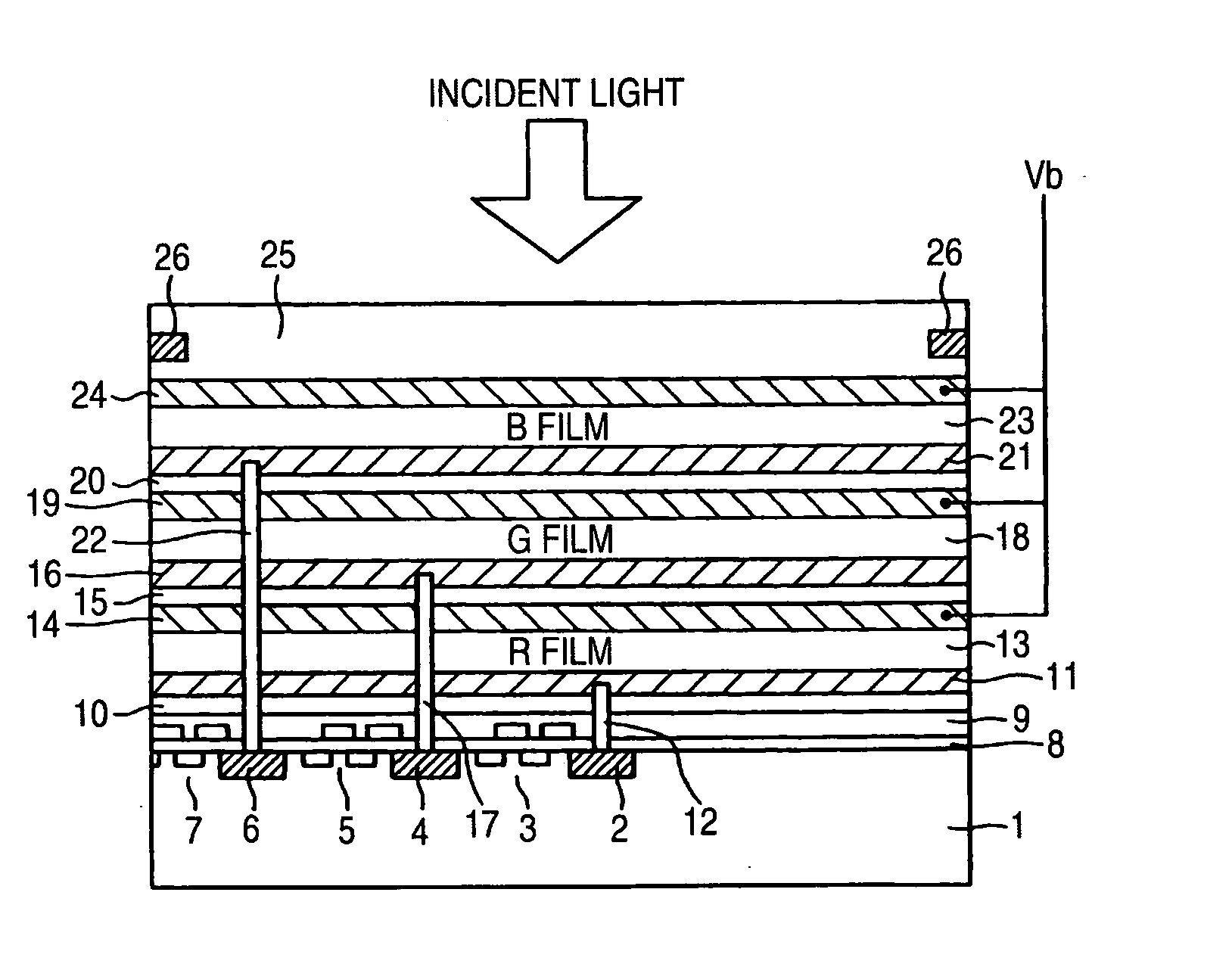
Figure 1 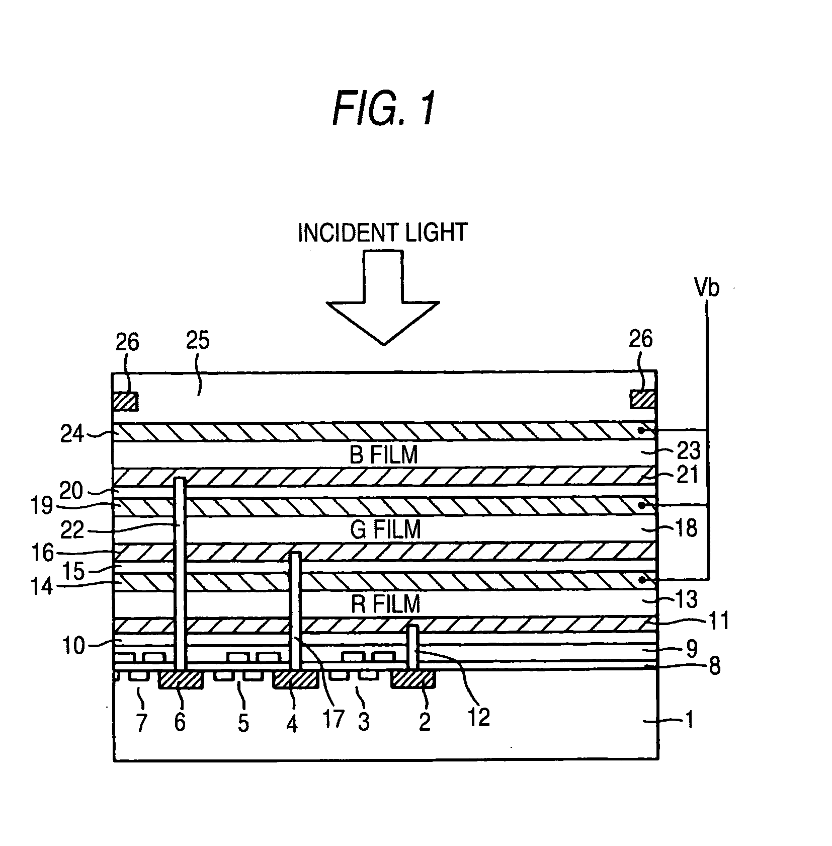
Figure 2 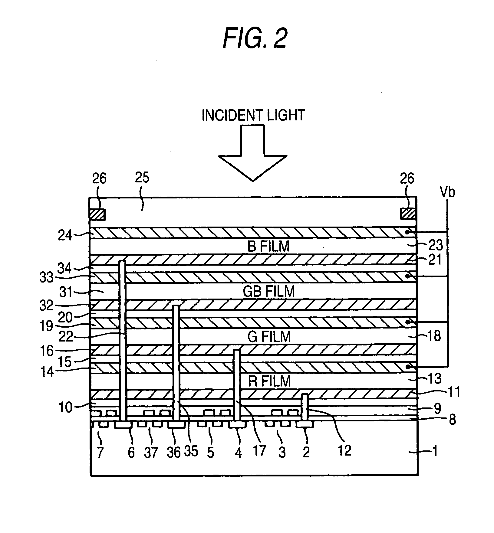
Figure 3
Abstract
Description
[0001] This is a divisional of application Ser. No. 11 / 080,539 filed Sep. 11, 2003, which claims priority from Japanese Patent Application No 2004-076068 filed on Mar. 17, 2004 the disclosures of which are incorporated by reference in their entirety.BACKGROUND OF THE INVENTION
[0002] 1. Field of the Invention
[0003] The present invention relates to a photoelectric converting film stack type solid-state image pickup device fabricated by stacking a photoelectric converting film on a semiconductor substrate having formed on the surface thereof a signal read circuit.
[0004] 2. Description of the Related Art
[0005] As for the photoelectric converting film stack type solid-state image pickup device, a prototype device is described, for example, in JP-A-58-103165. In this solid-state image pickup device, three photosensitive layers are stacked on a semiconductor substrate, and electrical signals of red (R), green (G) and blue (B) detected by respective photosensitive layers are read out by MOS circ...
Examples
Embodiment Construction
[0045]One embodiment of the present invention is described below by referring to the drawings.
[0046]FIG. 1 is a cross-sectional schematic view of one pixel portion of the photoelectric converting film stack type solid-state image pickup device according to one embodiment of the present invention. This embodiment takes a constitution such that photoelectric converting films are stacked in three layers to take out electrical signals corresponding to three primary colors of red (R), green (G) and blue (B), namely, a constitution of picking up a color image, but a constitution of picking up a monochromatic image, for example, a black-and-white image, by providing only one photoelectric converting film layer may also be employed.
[0047]In FIG. 1, a high-concentration impurity region 2 for accumulating the red color signal, an MOS circuit 3 for reading out the red color signal, a high-concentration impurity region 4 for accumulating the green signal, an MOS circuit 5 for reading out the gr...