
Method for fabricating semiconductor device
a semiconductor and device technology, applied in the direction of semiconductor devices, semiconductor/solid-state device details, electrical equipment, etc., can solve the problems of poor adhesion to the insulating film and metals, short circuit between the contacts and between the interconnects, and reduced adhesion, so as to achieve the effect of removing water more effectively
Patent Information
- Authority / Receiving Office
- US · United States
- Patent Type
- Applications(United States)
- Current Assignee / Owner
- Publication Date
- 2009-03-26
Smart Images
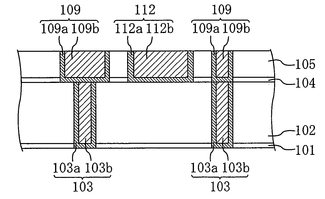
Figure 1 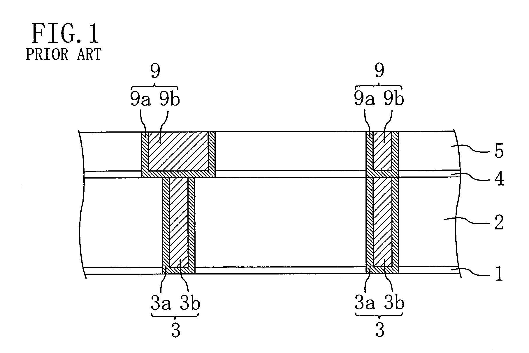
Figure 2 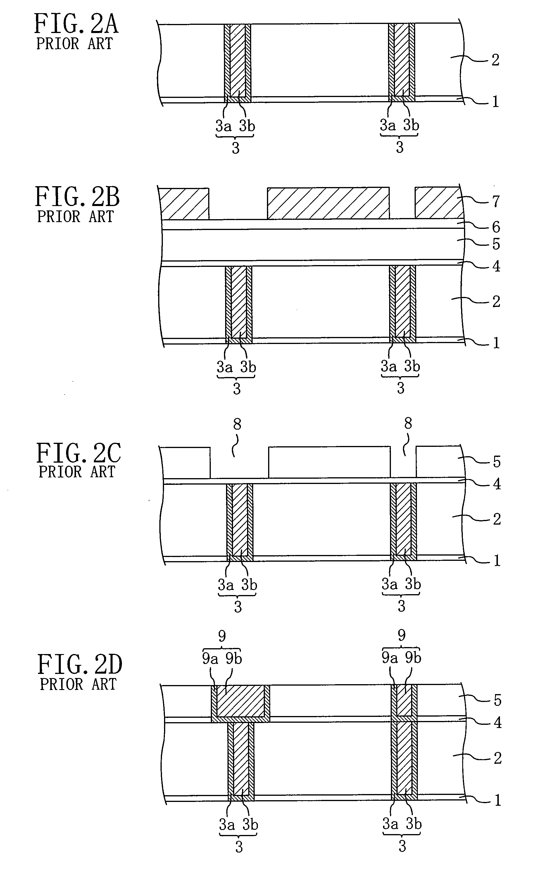
Figure 3
Abstract
Description
BACKGROUND OF THE INVENTION
[0001] 1. Field of the Invention
[0002] The present invention relates to a method for fabricating a semiconductor device, and more particularly relates to a technique for forming interconnects in a multilevel interconnection in which insulating films are formed between interconnect layers.
[0003] 2. Description of the Related Art
[0004] In recent years, miniaturization of semiconductor integrated circuits has been significantly advanced, and the degree of integration has been tremendously increasing. As the number of devices integrated on a single semiconductor integrated circuit has been increasing, delay time is expected to be reduced. However, in practice, although transistor delay time can be reduced, wiring resistance and parasitic capacitance are increased, making it difficult to reduce wiring delay time. In order to lower wiring resistance, instead of conventionally used aluminum, copper having a lower resistance is used as a wiring material. Also, in orde...
Examples
first embodiment
[0025]A method for fabricating a semiconductor device according to a first embodiment of the invention will be described with reference to FIGS. 3A to 3D.
[0026]First, as shown in FIG. 3A, contacts 103, each composed of a barrier metal film 103a and a metal film 103b, and dummy contacts 110, each composed of a barrier metal film 110a and a metal film 110b, are formed on a silicon substrate (not shown). To be specific, a first insulating film 101 is formed on the silicon substrate by a known method such as a CVD process. Then, a second insulating film 102, which is relatively high in moisture absorbency, is formed on the first insulating film 101. Next, a contact hole pattern made of a photoresist is formed on the second insulating film 102 by a photolithography process, and contact holes and dummy contact holes are formed by a dry etching process using this contact hole pattern. These dummy contact holes may or may not go through the second insulating film 102. Then, a heat treatment...
second embodiment
[0046]A method for fabricating a semiconductor device according to a second embodiment of the invention will be described with reference to FIGS. 6A to 6D. FIGS. 6A through 6D are cross-sectional views illustrating process steps in the semiconductor device fabrication method of this embodiment.
[0047]First, as shown in FIG. 6A, contacts 103, each composed of a barrier metal film 103a and a metal film 103b, are formed on a silicon substrate (not shown). To be specific, a first insulating film 101 is formed on the silicon substrate by a kwon method such as a CVD process. Then, a second insulating film 102 which is relatively high in moisture absorbency is formed on the first insulating film 101. Next, a contact hole pattern made of a photoresist is formed on the second insulating film 102 by a photolithography process, and contact holes are formed by a dry etching process using this contact hole pattern. Subsequently, a multilayer film made of tantalum nitride / tantalum or titanium / tita...