
Data transmitting system
a data transmission and data technology, applied in logic circuit coupling/interface arrangement, baseband system details, instruments, etc., can solve the problems of parasitic capacitor component in transmission lines, distortion of output signals, and increase parasitic capacitor components in transmission lines, so as to reduce signal coupling noise, shorten the transition time of signals, and inhibit the fluctuation of common mode voltage
Patent Information
- Authority / Receiving Office
- US · United States
- Patent Type
- Applications(United States)
- Current Assignee / Owner
- Publication Date
- 2010-05-20
- Estimated Expiration
- Not applicable · inactive patent
Smart Images
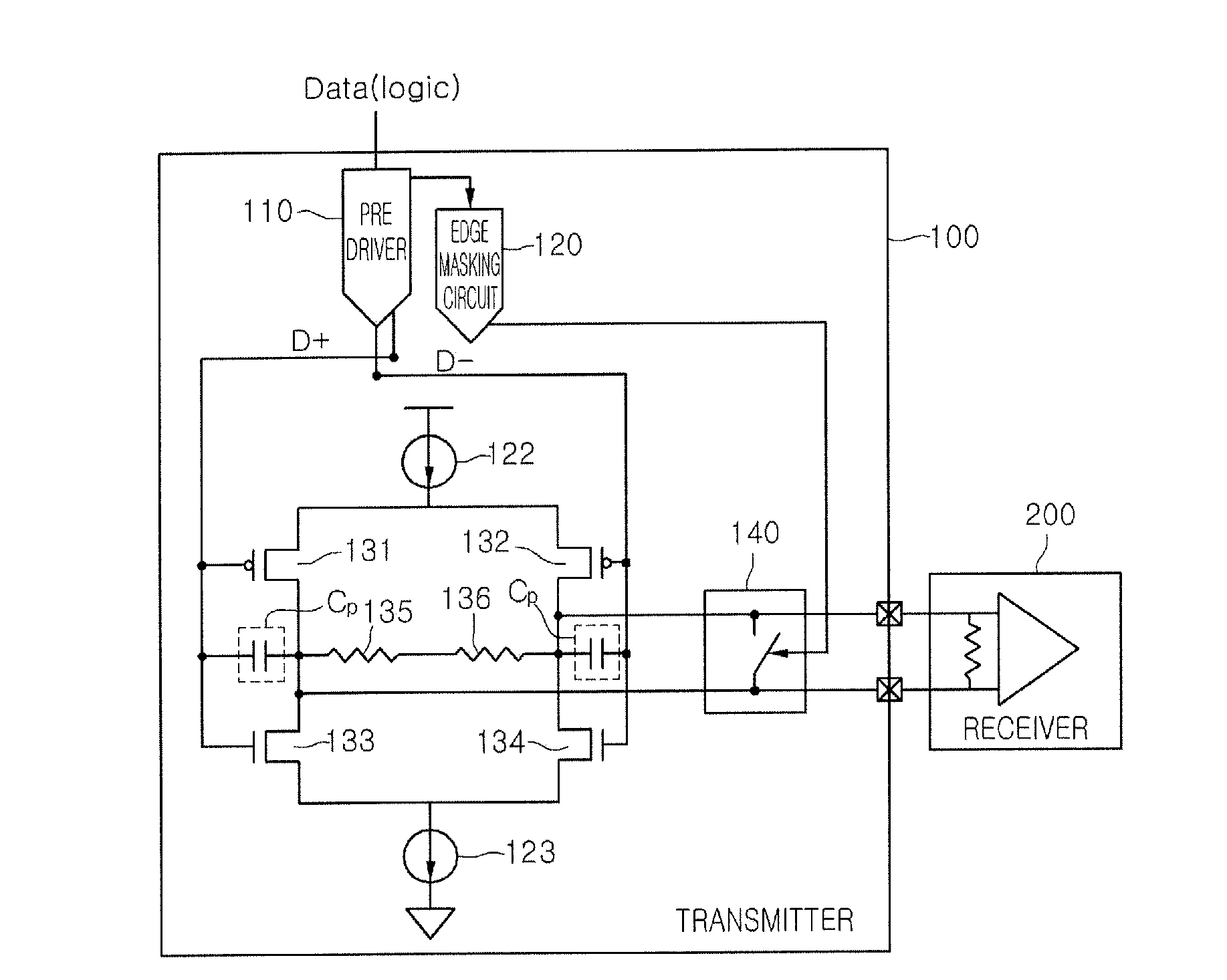
Figure 1 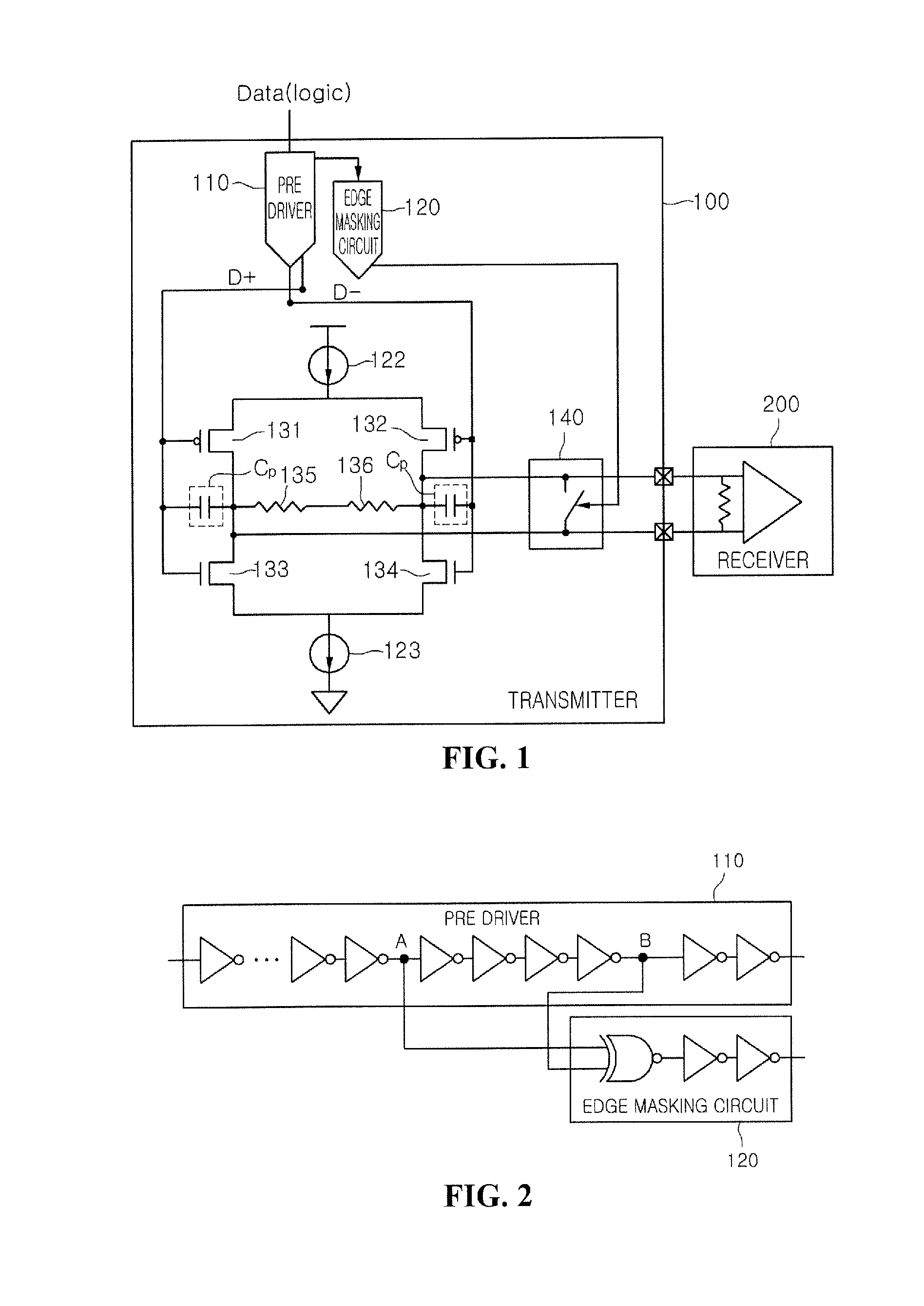
Figure 2 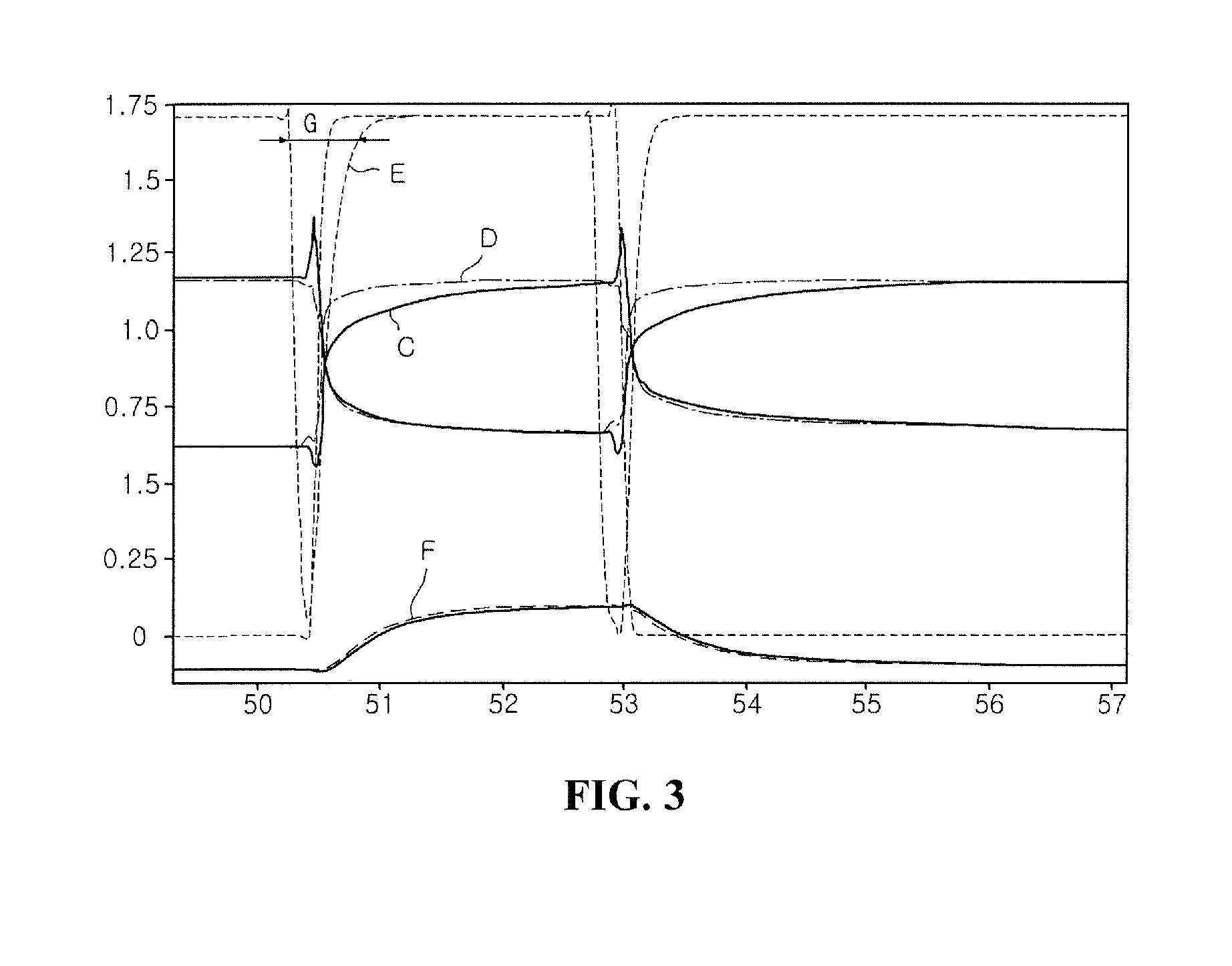
Figure 3
Abstract
Description
CROSS-REFERENCE TO RELATED APPLICATION
[0001] This application claims the benefit under 35 U.S.C. §119 of Korean Patent Application No. 10-2008-0113547, filed Nov. 14, 2008, which is hereby incorporated by reference in its entirety.BACKGROUND
[0002] Two schemes have typically been used when transmitting data through a transmission line that connects between two or more semiconductor chips.
[0003] The first scheme converts and transmits data signals into a difference in a current intensity that is output to the transmission line.
[0004] The second scheme converts data into a voltage difference at a transmitting side, carries the voltage difference on the transmission line, detects the voltage difference at a receiving side, and recovers the data.
[0005] The above-mentioned voltage driving scheme may be classified into a single voltage driving scheme that assigns one transmission line for each data according to the number of lines receiving one bit data and provides the data as the magnitude of...
Examples
Embodiment Construction
[0014]A data transmitting system according to an embodiment will be described in detail with reference to the accompanying drawings.
[0015]Hereinafter, the detailed description of a related known functions or configurations that may unnecessarily obscure the subject matter of the present invention in describing the present invention will be omitted. Therefore, only the core components, which are directly related with the technical idea of the present invention, will be described.
[0016]FIG. 1 is a block diagram of a data transmitting system according to an embodiment. FIG. 2 is a block diagram providing a more detailed view of a pre-driver 110 and an edge masking circuit 120 of a transmitter 100 in accordance with an embodiment of a data transmitting system.
[0017]In addition, FIG. 3 is a timing diagram graphically showing a signal form processed in the data transmitting system according to an embodiment.
[0018]Referring to FIG. 1, the data transmitting system according to an embodiment...