
Scannable synchronizer having a deceased resolving time
a synchronizer and dead technology, applied in the field of synchronizers, can solve the problems of limiting the speed of the master latch, and providing no gain to the signals, so as to reduce the resolving time associated with the master latch, reduce the possibility, and reduce the transition time of the input data signal
Patent Information
- Authority / Receiving Office
- US · United States
- Patent Type
- Patents(United States)
- Current Assignee / Owner
- Publication Date
- 2005-05-17
- Estimated Expiration
- Not applicable · inactive patent
Smart Images
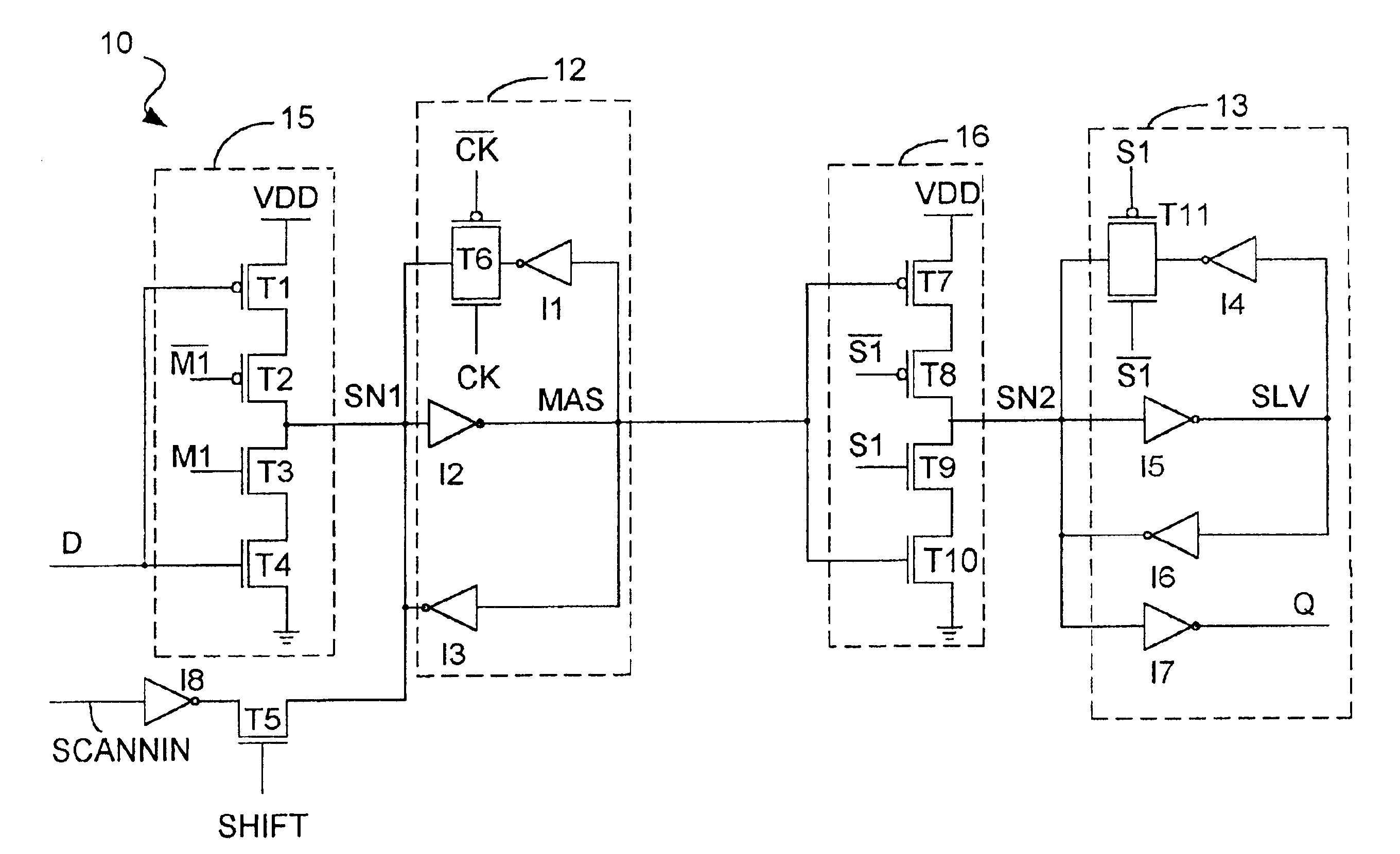
Figure 1 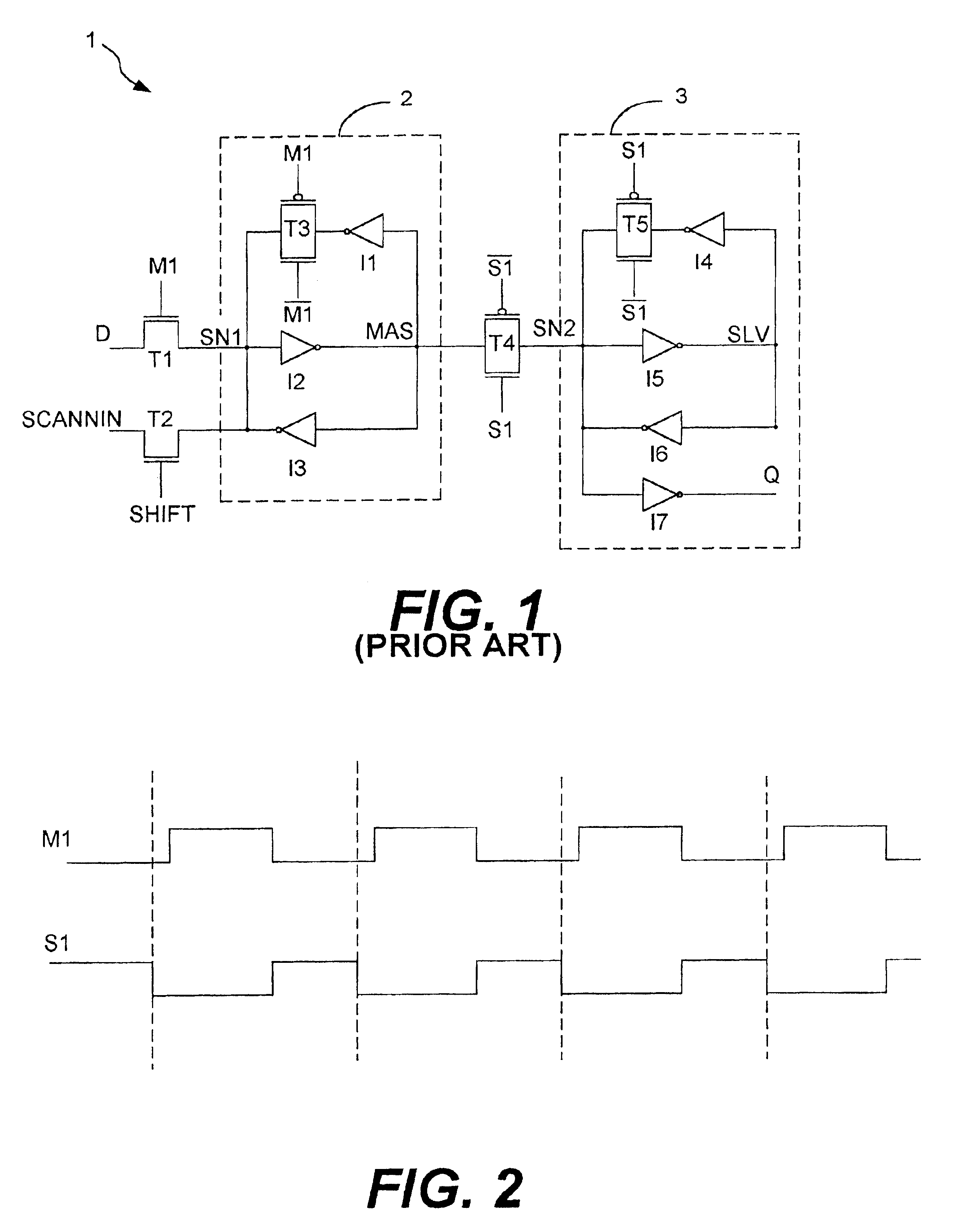
Figure 2 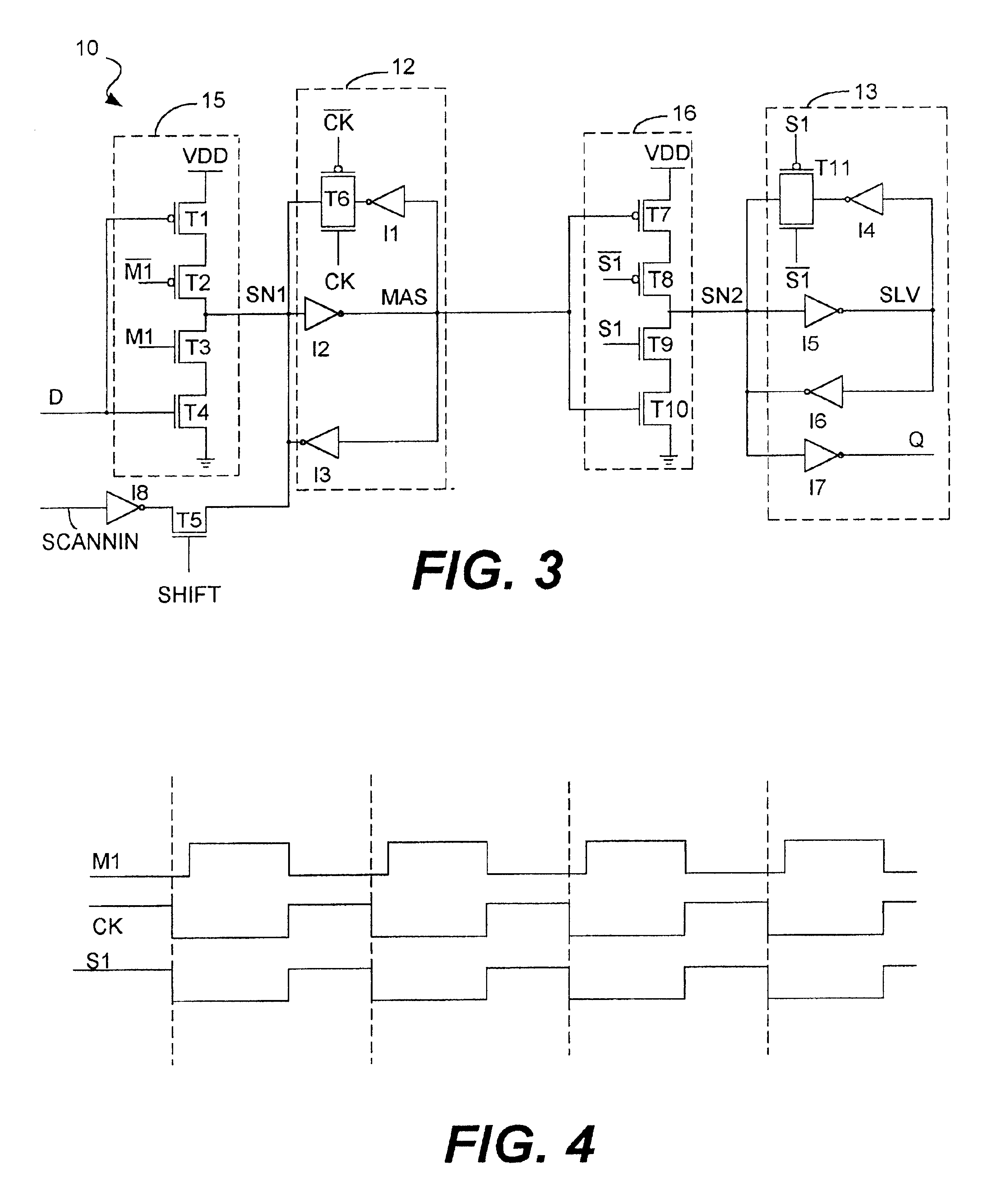
Figure 3
Abstract
Description
TECHNICAL FIELD OF THE INVENTION
[0001] The present invention relates generally to synchronizers and, more particularly, to a scannable synchronizer having an improved design that enables the resolving time associated with the synchronizer to be decreased and that decreases the likelihood that a synchronizer failure will occur.BACKGROUND OF THE INVENTION
[0002] Synchronizers receive data from upstream logic in one clock domain and synchronize that data to another clock domain associated with logic downstream of the synchronizer. The synchronizer ensures that the data coming out of the synchronizer will not violate the setup or hold constraints of clocked elements located downstream of the synchronizer. During synchronization, it is possible for the incoming data to violate the setup or hold constraints of the synchronizer itself, and thereby cause a meta-stable condition to occur in the synchronizer. The amount of time that it takes for the synchronizer to exit this meta-stable state an...
Examples
Embodiment Construction
[0024]FIG. 3 is a schematic diagram of the synchronizer 10 of the present invention in accordance with the preferred embodiment. The synchronizer 10 comprises a master latch 12 and a slave latch 13. The master and slave latches 12 and 13 operate in a manner that is substantially identical to the manner in which the master and slave latches 2 and 3, respectively, shown in FIG. 1 operate. However, the synchronizer 10 of the present invention utilizes an input stage 15 to the master latch 12 and an input stage 16 to the slave latch 13 that are clocked inverters that facilitate the resolving processes performed by the master and slave latches 12 and 13, as described below in more detail. Therefore, the input stages 15 and 16 improve the resolving time of the synchronizer 10 and minimize the likelihood that a synchronizer failure will occur.
[0025]Another difference between the synchronizer 10 of the present invention and the synchronizer 1 shown in FIG. 1 is that the gate T6 is not contr...