
Silicon carbide substrate, semiconductor device, and methods for manufacturing them
a technology of silicon carbide substrate and semiconductor device, which is applied in the direction of crystal growth process, polycrystalline material growth, chemistry apparatus and processes, etc., can solve the problems of deterioration of the characteristics inhibiting epitaxial growth, and affecting so as to improve the manufacturing efficiency of the semiconductor device, reduce the effect of manufacturing cos
Patent Information
- Authority / Receiving Office
- US · United States
- Patent Type
- Applications(United States)
- Current Assignee / Owner
- Publication Date
- 2013-10-03
Smart Images
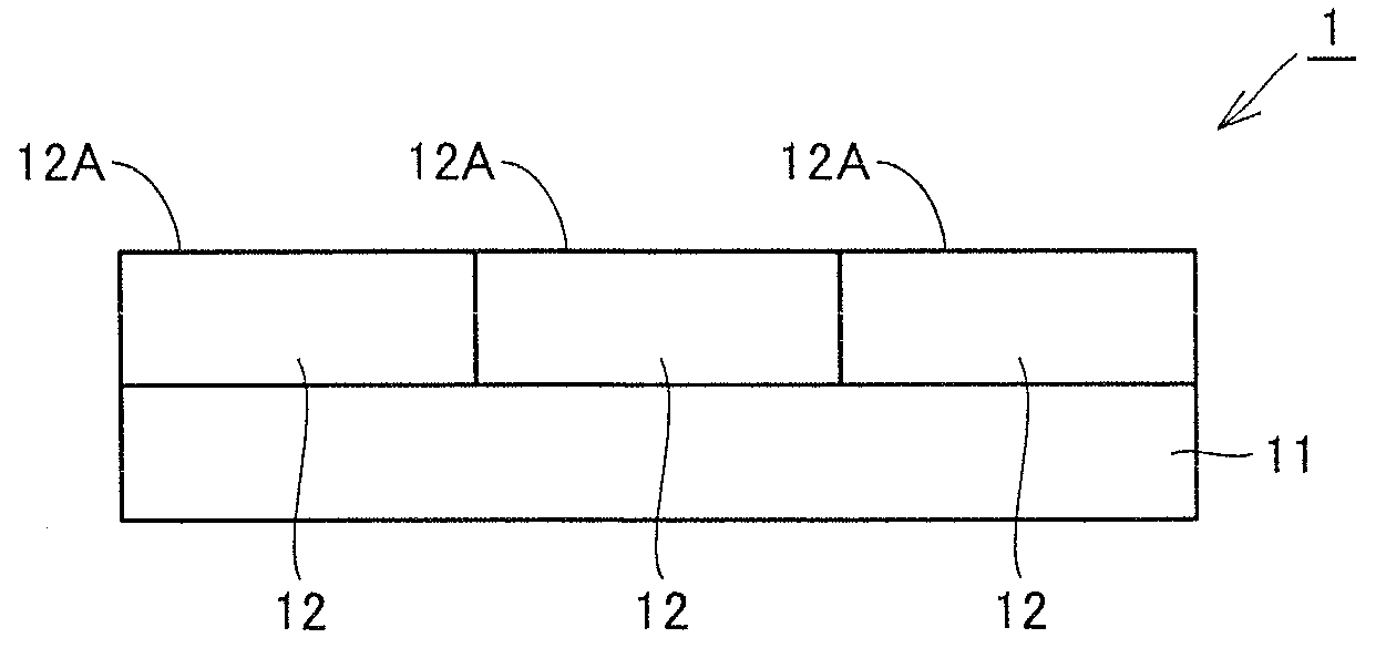
Figure 1 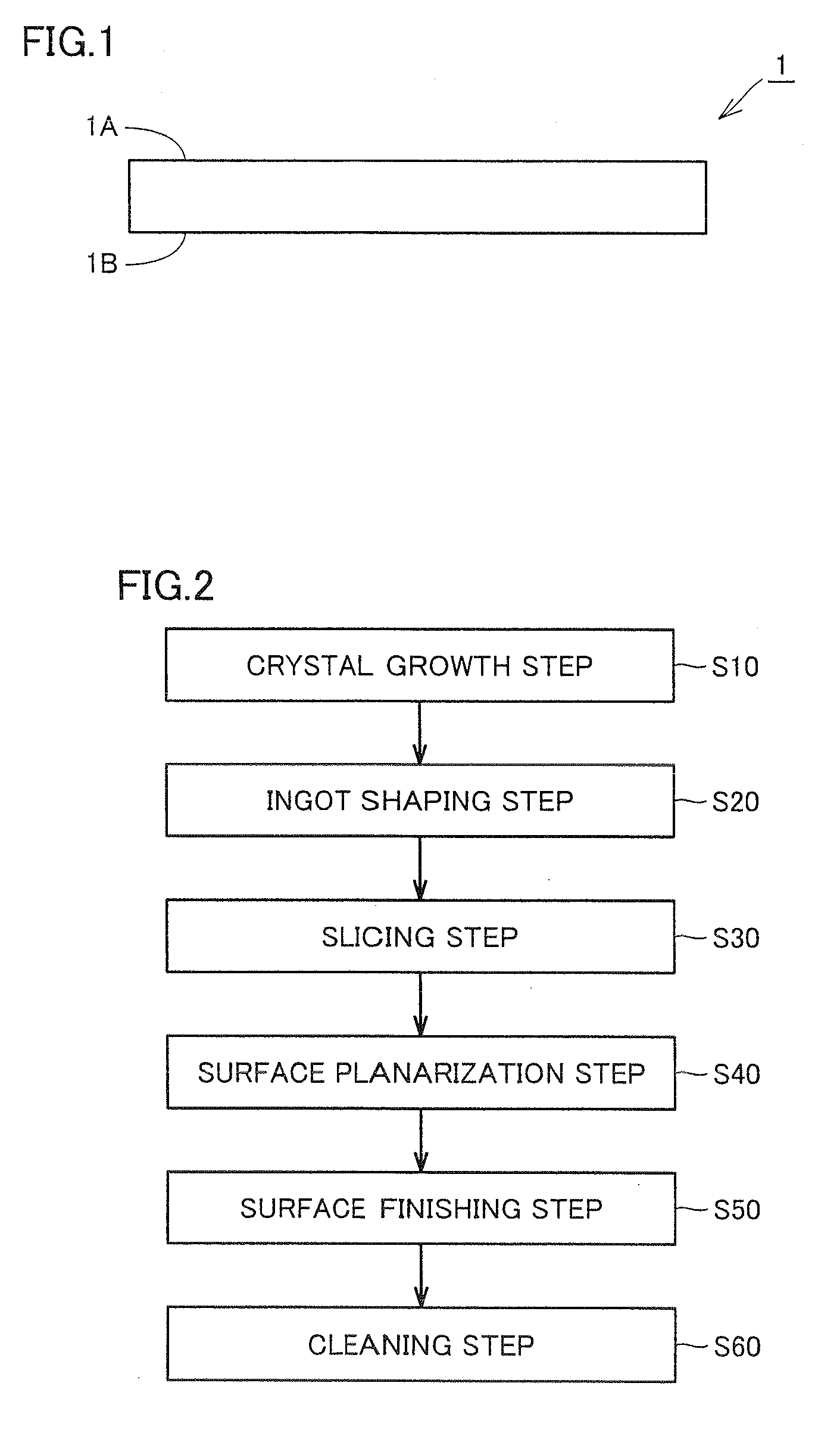
Figure 2 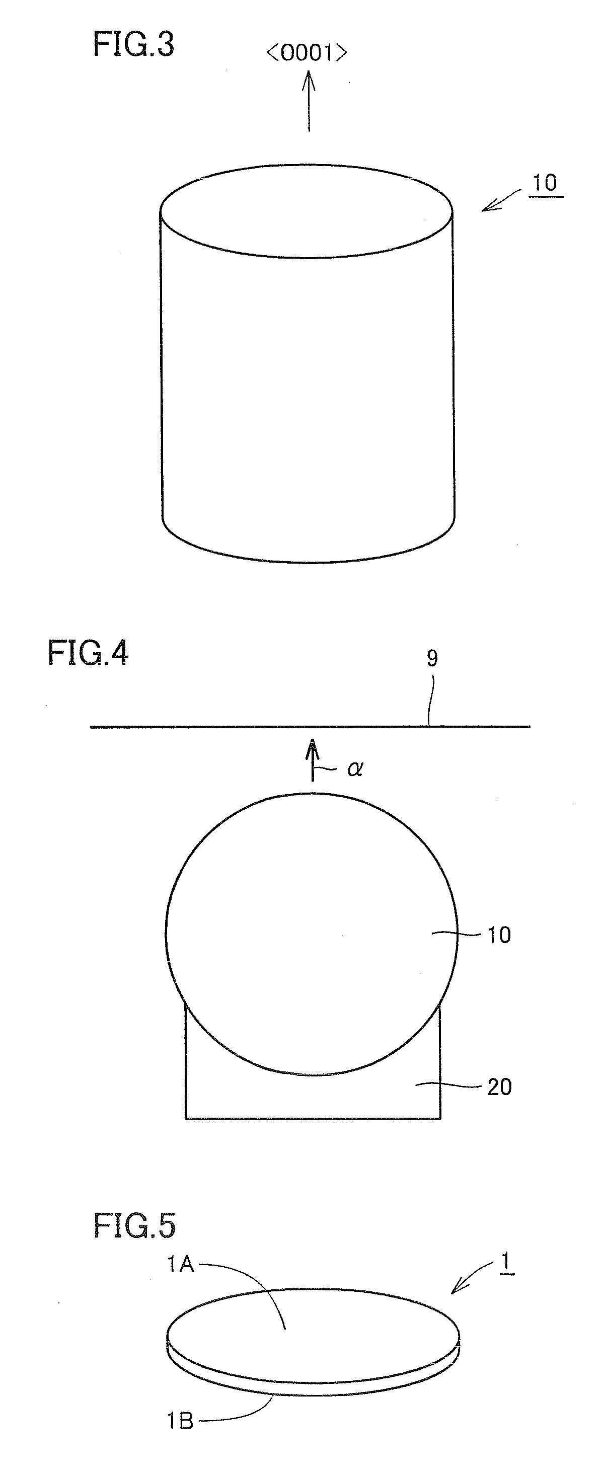
Figure 3
Abstract
Description
BACKGROUND OF THE INVENTION
[0001] 1. Field of the Invention
[0002] The present invention relates to a silicon carbide substrate, a semiconductor device, and methods for manufacturing them. More particularly, the present invention relates to a silicon carbide substrate capable of improving yield of semiconductor device characteristics, a semiconductor device using the substrate, and methods for manufacturing them.
[0003] 2. Description of the Background Art
[0004] In recent years, in order to achieve higher breakdown voltage and lower loss of a semiconductor device, use thereof in a high temperature environment, and the like, silicon carbide has increasingly been adopted as a material for forming a semiconductor device. Since silicon carbide is excellent in heat conductivity when compared with a semiconductor made of a nitride such as gallium nitride, it is excellent as a substrate for a semiconductor device for high-power application at high voltage and large current.
[0005] In order to form...
Examples
first embodiment
[0050]First, a silicon carbide substrate as one embodiment of the present invention will be described. Referring to FIG. 1, a silicon carbide substrate 1 in the present embodiment is entirely made of single-crystal silicon carbide, and has a first main surface 1A and a second main surface 1B opposite to the first main surface. In at least one main surface of first and second main surfaces 1A and 1B (for example, first main surface 1A), sulfur atoms are present at not less than 60×1010 atoms / cm2 and not more than 2000×1010 atoms / cm2, and carbon atoms as an impurity are present at not less than 3 at % and not more than 25 at %.
[0051]Since the presence ratio of the sulfur atoms is not less than 60×1010 atoms / cm2 and the presence ratio of the carbon atoms as the impurity is not less than 3 at %, the silicon carbide substrate has a stabilized surface. In addition, since the presence ratio of the sulfur atoms is not more than 2000×1010 atoms / cm2 and the presence ratio of the carbon atoms ...
second embodiment
[0087]Next, a silicon carbide substrate in a second embodiment will be described. Referring to FIG. 8, silicon carbide substrate 1 in the second embodiment basically has the same structure and exhibits the same effect as those of silicon carbide substrate 1 in the first embodiment. However, silicon carbide substrate 1 in the second embodiment is different from that in the first embodiment in that it includes a base layer 11 and a single-crystal silicon carbide layer 12.
[0088]Specifically, referring to FIG. 8, silicon carbide substrate 1 in the second embodiment includes base layer 11, and single-crystal silicon carbide layer 12 formed on base layer 11. Further, a main surface 12A of single-crystal silicon carbide layer 12 on a side opposite to a side facing base layer 11 corresponds to main surface 1A in the first embodiment. That is, in silicon carbide substrate 1 in the present embodiment, a region including one main surface 12A is made of single-crystal silicon carbide. The prese...
example 1
[0095]An experiment was conducted to investigate the influence of the presence ratios of sulfur atoms and carbon atoms as an impurity in a main surface of a silicon carbide substrate on yield of a semiconductor device.
[0096]A silicon carbide single crystal was grown by the sublimation method. Silicon carbide substrate 1 with a diameter of 80 mm was used as a seed substrate. The seed substrate had a main surface corresponding to a (0001) plane. A grown surface, an underlying substrate surface, and an outer periphery of the silicon carbide single crystal were ground with an outer periphery grinding machine to obtain an ingot of the silicon carbide single crystal. Slicing of the ingot was performed using a multiwire saw. The ingot was cut such that a main surface of sliced silicon carbide substrate 1 (hereinafter also referred to as a surface) would serve as a surface that was 4° off from the (0001) plane. Sliced silicon carbide substrate 1 had a thickness of 400 μm. Silicon carbide su...