
Semiconductor device and method for producing the same
Patent Information
- Authority / Receiving Office
- US · United States
- Current Assignee / Owner
- Publication Date
- 2014-03-13
Smart Images
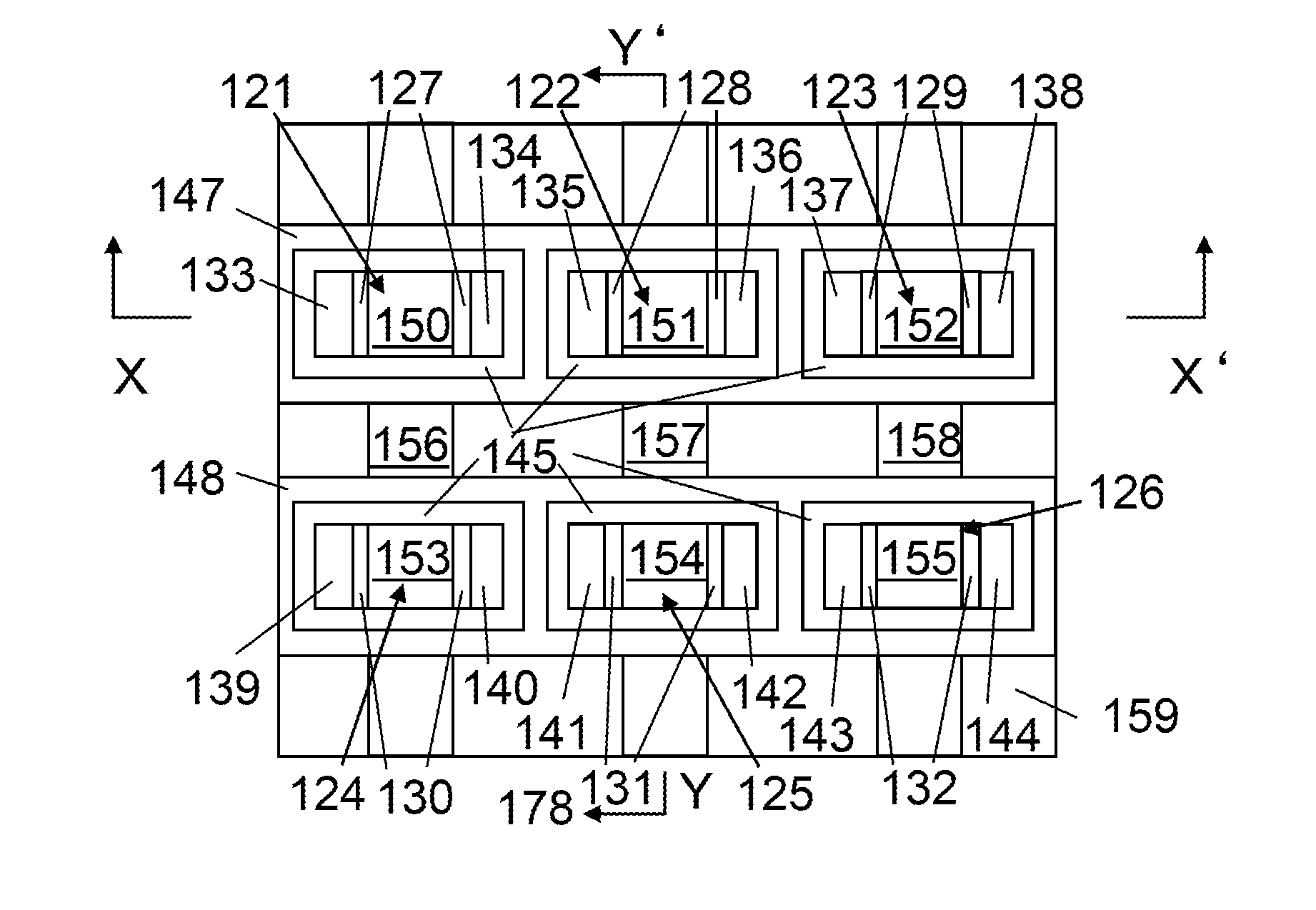
Figure 1 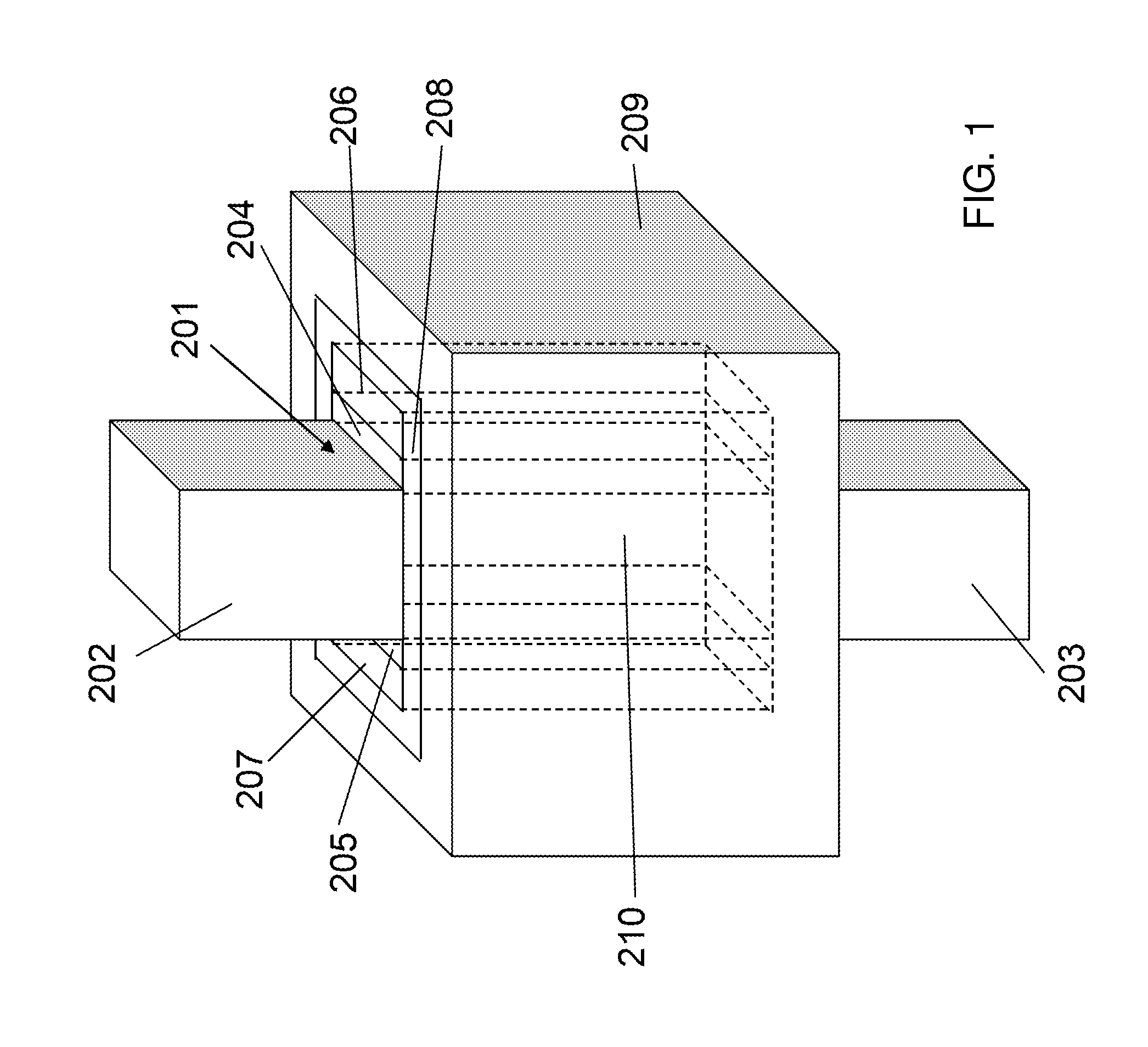
Figure 2 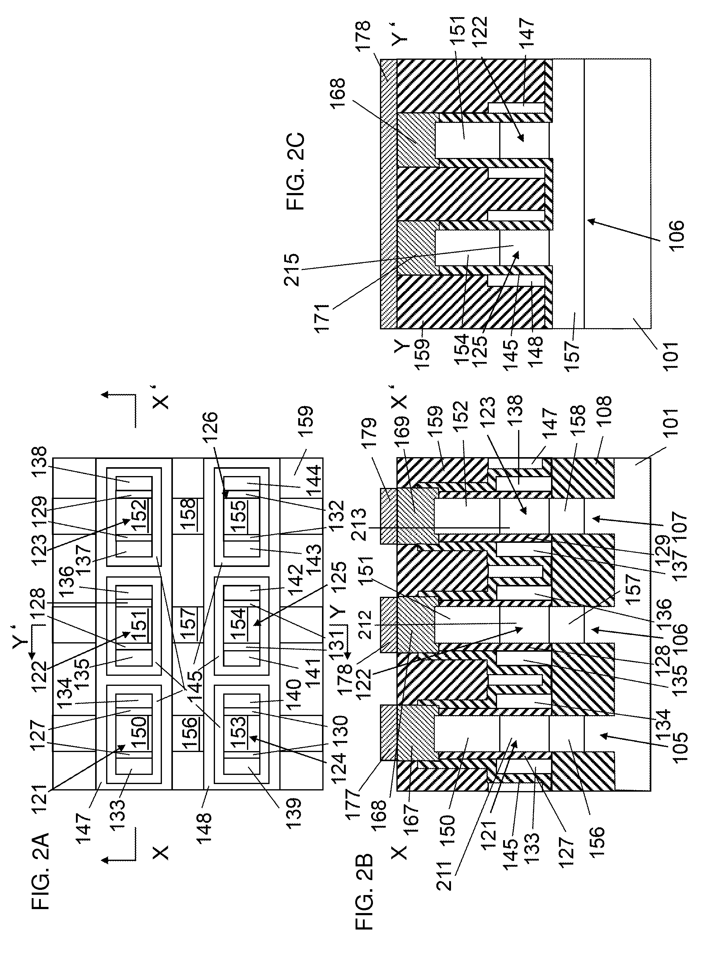
Figure 3
Abstract
Description
CROSS REFERENCE TO RELATED APPLICATION
[0001] This application claims the benefit, under 35 U.S.C. §119(e), of provisional patent application No. 61 / 698,054, filed Sep. 7, 2012; the contents of the prior application are herewith incorporated by reference.BACKGROUND OF THE INVENTION
[0002] 1. Field of the Invention
[0003] The present invention relates to a semiconductor device and a method for producing the semiconductor device.
[0004] 2. Description of the Related Art
[0005] There has been proposed a flash memory that includes a memory cell including a floating gate and a control gate formed on a side wall of a pillar-shaped semiconductor layer, which is formed on a surface of a semiconductor substrate, so as to surround the pillar-shaped semiconductor layer. In this flash memory, the capacitance between the floating gate and the control gate can be increased with a small area occupied on the substrate, and the flash memory has high writing and erasing efficiencies (e.g., refer to Japanese Un...
Examples
Embodiment Construction
[0058]A semiconductor device according to an embodiment of the present invention will now be described with reference to the attached drawings. It should be understood that the scope of the present invention is not limited to the embodiment described below.
[0059]As shown in FIG. 1, the semiconductor device according to this embodiment includes a quadrangular pillar-shaped semiconductor layer 201 that extends in a vertical direction (Z-axis direction), the pillar-shaped semiconductor layer 201 including a first diffusion layer 203, a channel region 210, and a second diffusion layer 202 formed in that order from the substrate side. Floating gates 206 and 207 are respectively disposed in two symmetrical directions (along two parallel straight lines that extend along a Z axis and are provided using the pillar-shaped semiconductor layer 201 as the center) so as to sandwich the pillar-shaped semiconductor layer 201. A control gate line 209 is disposed in two other symmetrical directions (...