
Method for forming metal wiring in semiconductor device
Patent Information
- Authority / Receiving Office
- US · United States
- Current Assignee / Owner
- Publication Date
- 2005-06-30
- Estimated Expiration
- Not applicable · inactive patent
Smart Images
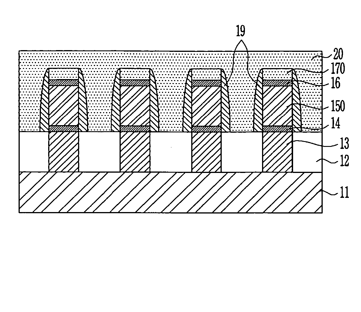
Figure 1 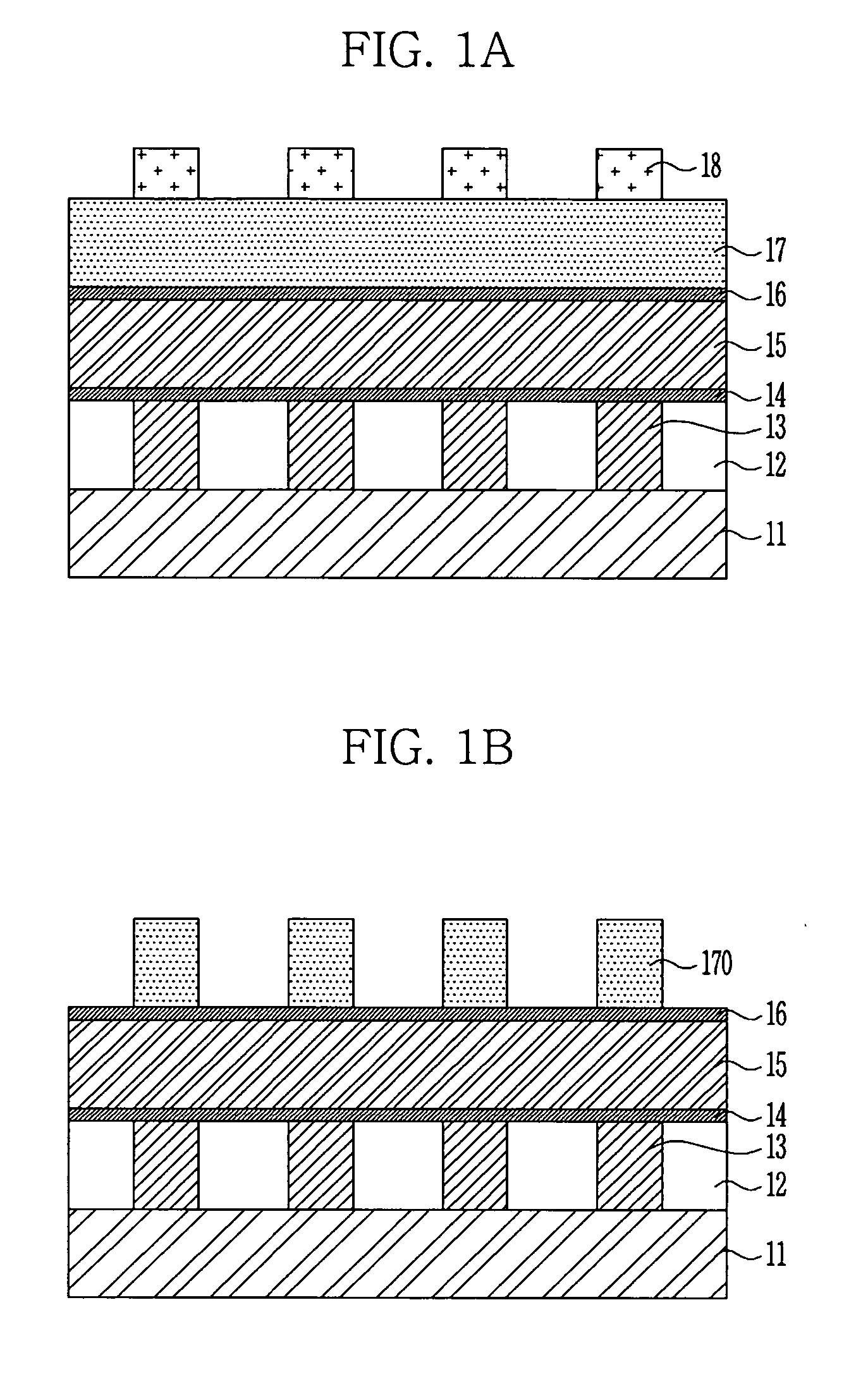
Figure 2 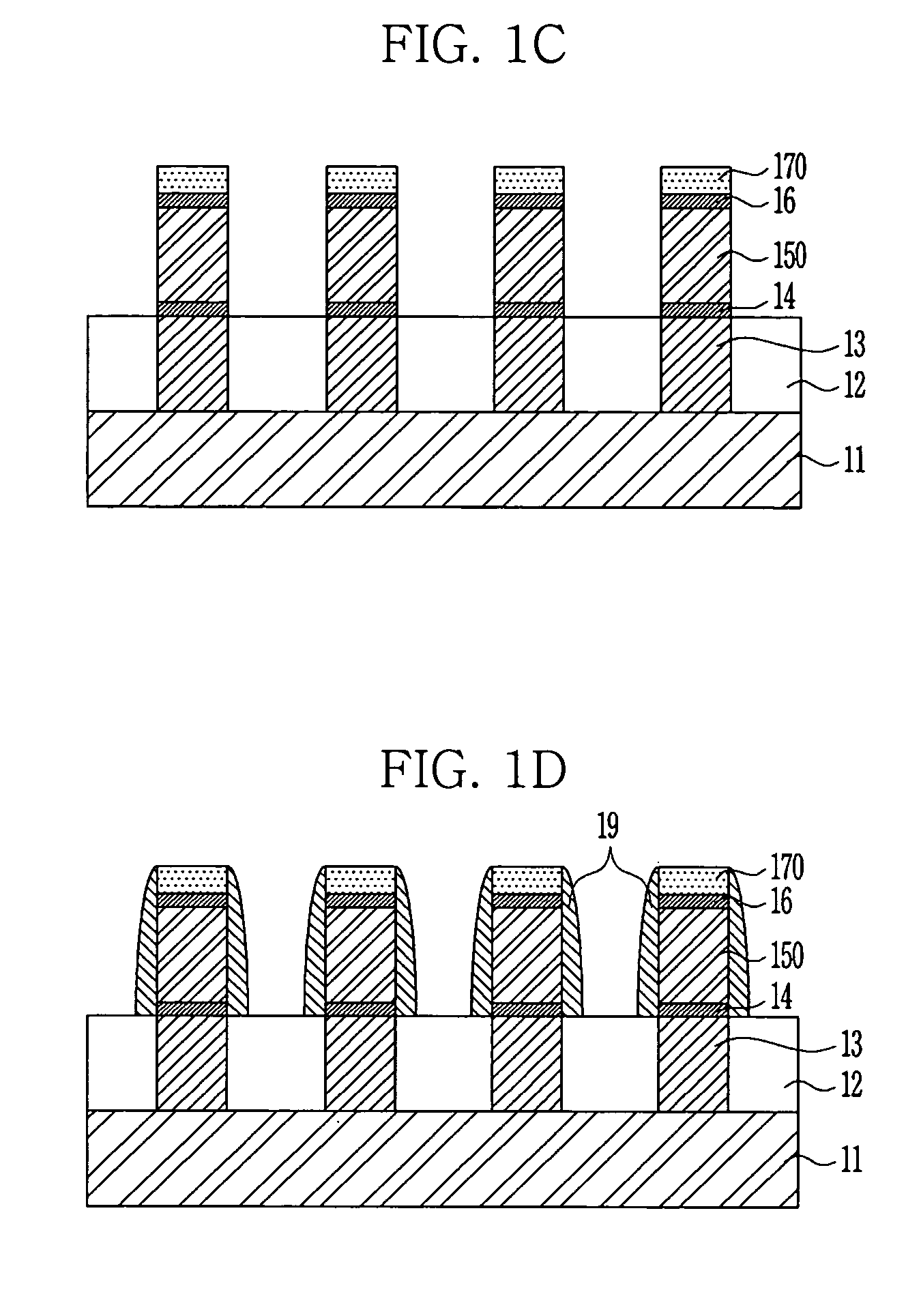
Figure 3
Abstract
Description
BACKGROUND
[0001] 1. Field of the Invention
[0002] The present invention relates to a method for forming metal lines in a semiconductor device, and more particularly to, a method for forming metal lines in a semiconductor device which can reduce an RC delay time by restricting crosstalk between the metal lines and decreasing capacitance between the metal lines, by using a low-k dielectric layer and performing a reactive ion etching (RIE) process.
[0003] 2. Discussion of Related Art
[0004] According to a high integration, high function and miniaturization tendency of a semiconductor device, a material which is advantageous in an RC delay time due to a low specific resistance, and which is highly resistible to electromigration (EM) and stressmigration (SM) is required as a material of metal lines. Instead of Al which has been generally used as the most appropriate material of the metal lines, Cu newly attracts attention.
[0005] Cu is used as the material of the metal lines because a m...
Examples
Embodiment Construction
[0021] A method for forming metal lines in a semiconductor device in accordance with a preferred embodiment of the present invention will now be described in detail with reference to the accompanying drawings.
[0022] In case it is described that one film is disposed on or contacts another film or a semiconductor substrate, one film can directly contact another film or the semiconductor substrate, or the third film can be positioned between them. In the drawings, a thickness or size of each layer may be exaggerated to provide easy and clear explanations. Wherever possible, the same reference numerals will be used throughout the drawings and the description to refer to the same or like parts.
[0023]FIGS. 1A to 1E are cross-sectional diagrams illustrating sequential steps of the method for forming the metal lines in the semiconductor device in accordance with the preferred embodiment of the present invention.
[0024] Referring to FIG. 1A, a first interlayer insulation film 12 is formed ...