
Semiconductor photodiode device and manufacturing method thereof
Patent Information
- Authority / Receiving Office
- US · United States
- Current Assignee / Owner
- Publication Date
- 2011-02-10
- Estimated Expiration
- Not applicable · inactive patent
Smart Images
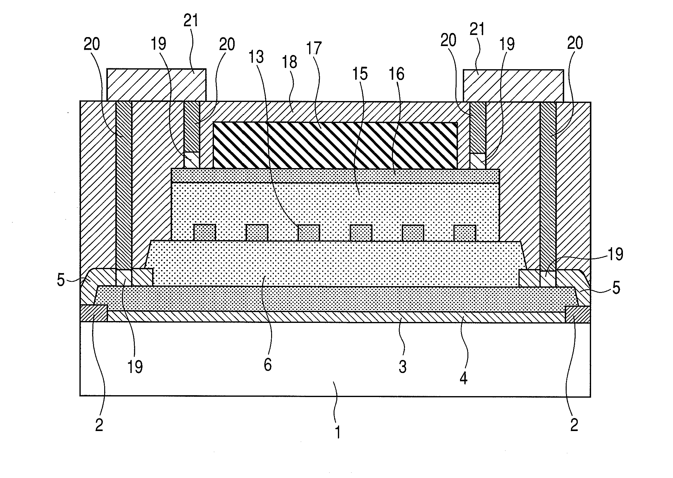
Figure 1 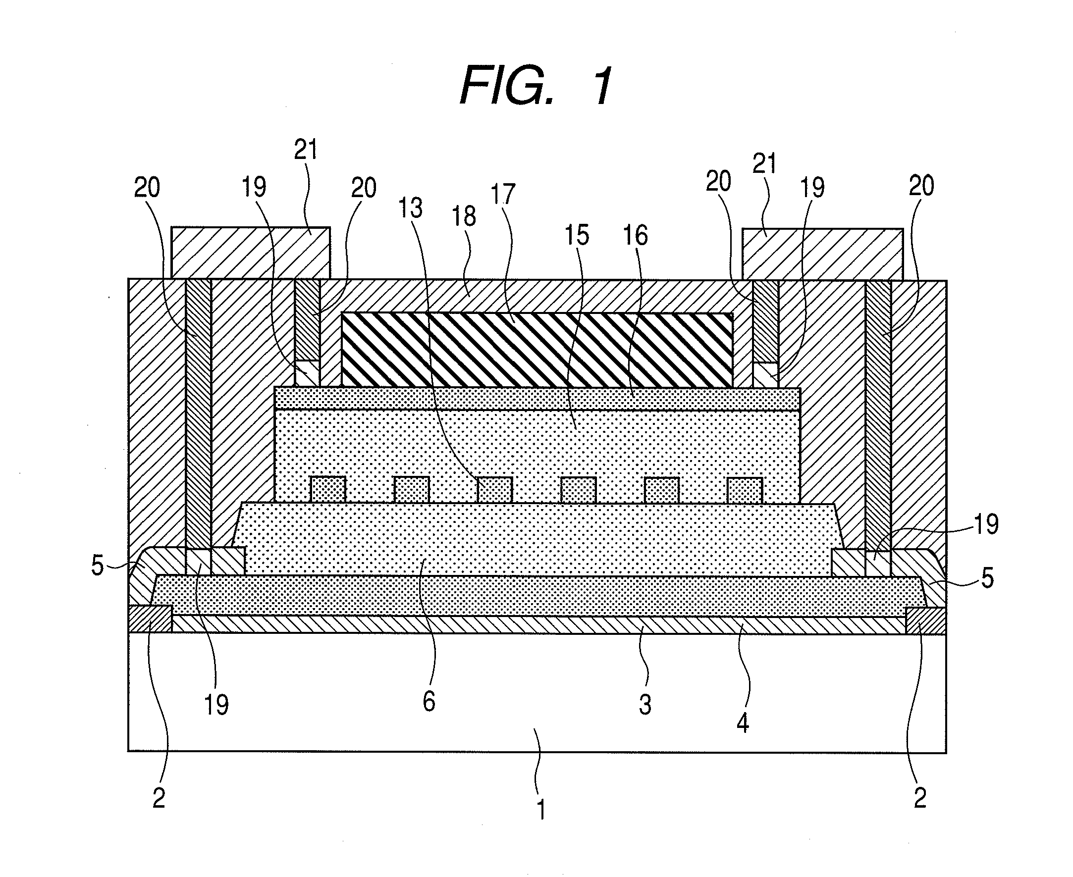
Figure 2 
Figure 3
Abstract
Description
CLAIM OF PRIORITY
[0001] The present application claims priority from Japanese patent application JP 2009-184003 filed on Aug. 7, 2009, the content of which is hereby incorporated by reference into this application.FIELD OF THE INVENTION
[0002] The present invention relates to a semiconductor photodiode device which is a photodiode device using a germanium containing semiconductor and a manufacturing method thereof, and it particularly relates to a semiconductor photodiode device such as a germanium-phototransistor having a high sensitivity and a high speed performance, as well as a manufacturing method thereof.BACKGROUND OF THE INVENTION
[0003] In existent semiconductor photodiode devices, there has been a technique for overcoming a trade-off relation of the thickness and the inter-p / n electrode distance required for the photoreceiving portion thereby attaining both high speed performance and high efficiency performance (for example, refer to JP-T-2007-527626).
[0004] Further, in existent ...
Examples
first embodiment
[0104]FIG. 1 is a cross sectional view showing a first embodiment of a semiconductor photodiode device according to the invention. This cross sectional structure shows a cross section of a photoreceiving portion in a bipolar phototransistor having a photoreceiving portion and an amplification portion separately.
[0105]FIG. 1 shows a silicon substrate 1 and an insulating film 2 having a trench. Above the insulation film 2, an n-type Ge layer 4 is formed by way of a buffer layer 3 for improving the crystallinity of upper layers. A high resistance Ge layer 6 is formed within the trench formed with an insulating film 5 above the Ge layer 4, and a p-type Ge layer 13 divided at a predetermine distance in the direction horizontal to the substrate and a high resistance Ge layer 15 are formed in the layer thereabove. An n-type Ge layer 16 is formed above the high resistance Ge layer 15. A silicon nitride film (Si3N4) 17 and an interlayer insulating film 18 are also shown. Metal electrode 19 t...
second embodiment
[0117]FIG. 8A to FIG. 8D are views for the cross sectional structure showing a second embodiment of a semiconductor photodiode according device to the invention along a photodiode device manufacturing steps. In FIG. 8A to FIG. 8D, portions having same functions as those in the first embodiment carry identical references with those in the first embodiment. The manufacturing steps are to be described sequentially.
[0118]At first, an insulating film 22 is deposited above an Si substrate 1, and patterning is applied to remove the insulating film 22 by etching while leaving a predetermined region. Further, an insulating film 23 is deposited and a trench is formed to the insulating film 22 to obtain a structure shown in FIG. 8A. It is preferred to use, for example, Si3N4 for the insulating film 22 and use, for example, SiO2 for the insulating film 23. In this case, the Si3N4 film 22 may be fabricated by dry etching using sulfur hexafluoride (SF6) and the SiO2 film 23 may be fabricated by d...
third embodiment
[0123]This embodiment discloses a photodiode device structure in which the capacitance of the bipolar portion in the photodiode device is decreased, and the manufacturing method thereof. FIG. 9A to FIG. 9I are cross sectional views showing the manufacturing process of the semiconductor photodiode device in this embodiment. Drawings show cross sections including the bipolar portion. While only one bipolar portion is shown in FIG. 9A to FIG. 9I for avoiding complexity, the bipolar portion may be present also in the opposite direction of the photoreceiving portion putting the portion therebetween.
[0124]At first, after depositing an insulating film 22 over an Si substrate 1 as shown in FIG. 9A, patterning is applied to leave the insulating film 22 while leaving only for the electrode fainting portions of the collector region in the bipolar portion and the n-type Ge layer in the photoreceiving portion and eliminating the remaining portions by etching. In the same manner as in the second ...