
Passive amplification circuit and analog-digital convertor
Patent Information
- Authority / Receiving Office
- US · United States
- Current Assignee / Owner
- Publication Date
- 2014-07-24
Smart Images
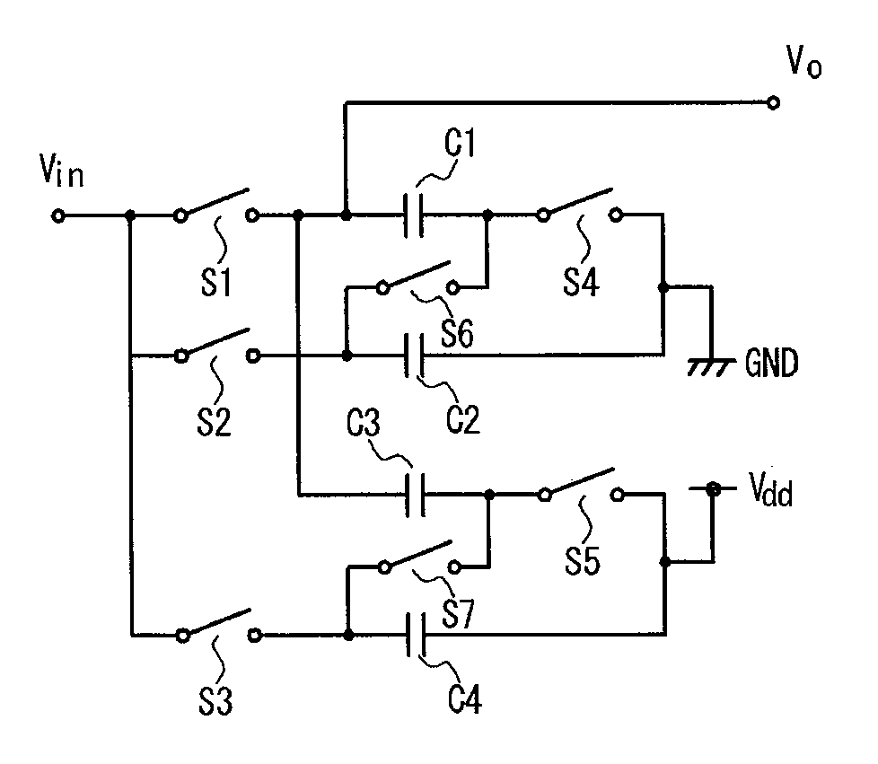
Figure 1 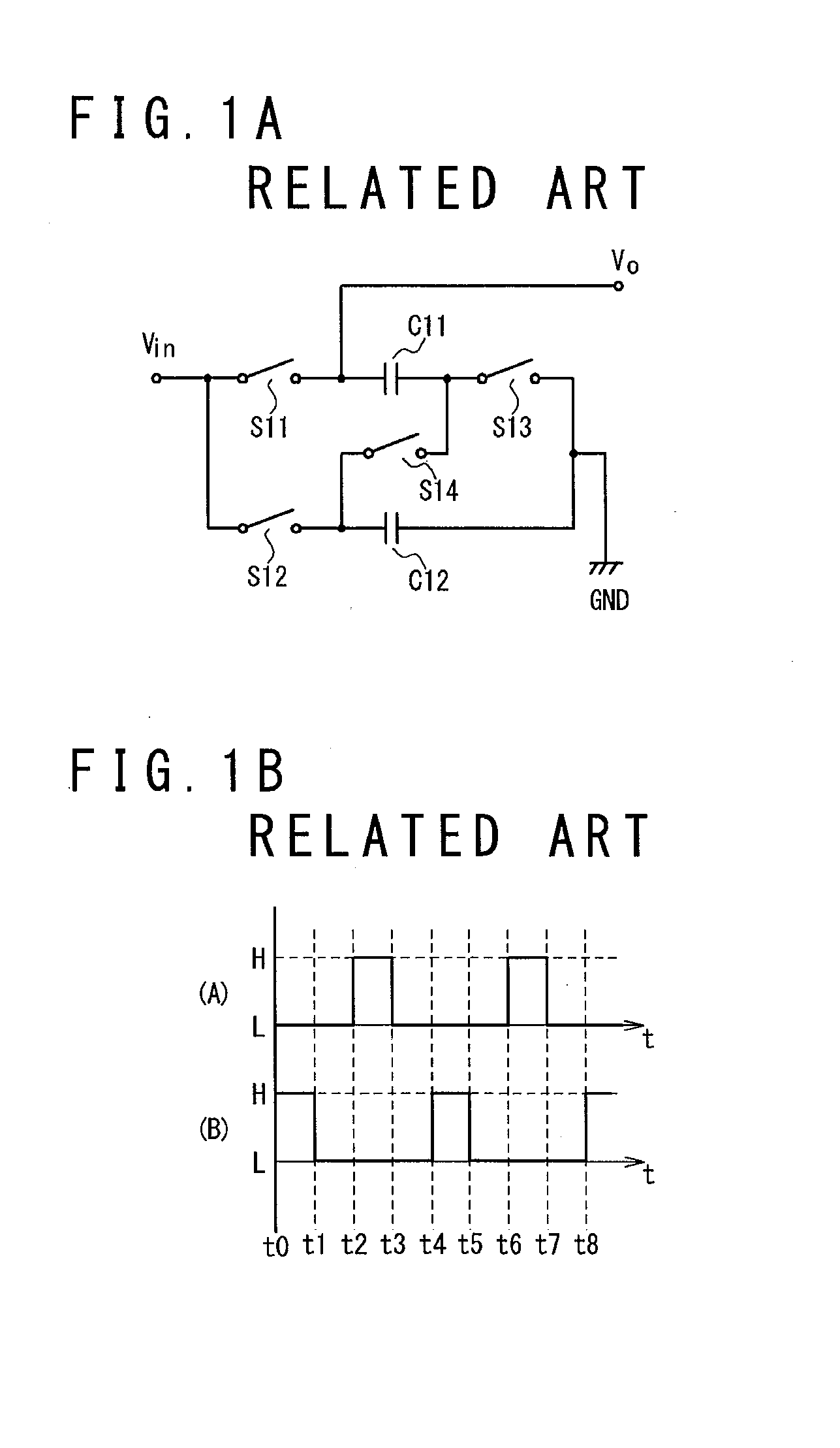
Figure 2 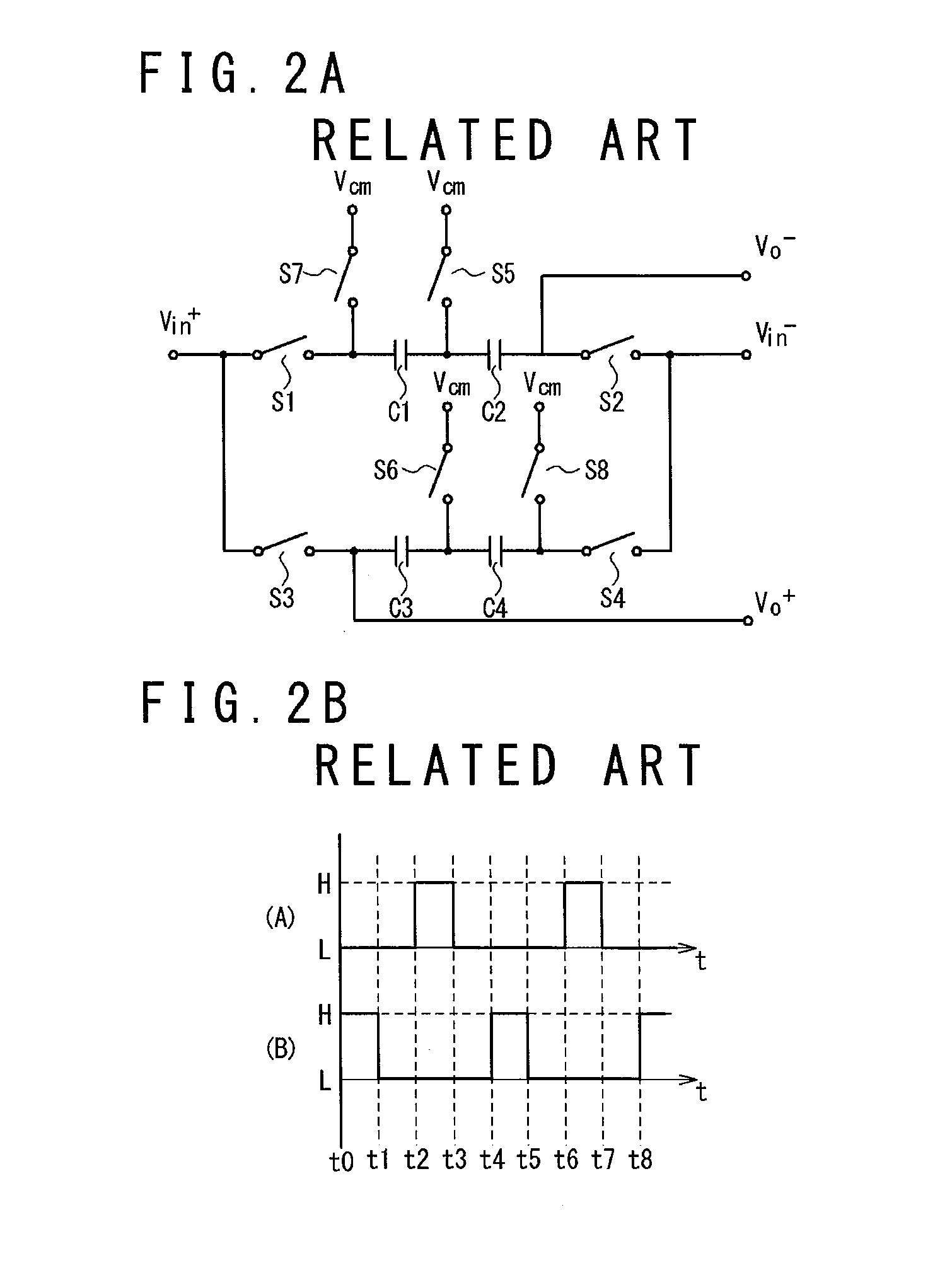
Figure 3
Abstract
Description
[0001] This application claims priorities on convention based on Japanese Patent Application Nos. JP 2013-010218 and JP 2013-259954. The disclosure thereof is incorporated herein by reference.TECHNICAL FIELD
[0002] The present invention is related to a passive amplification circuit and an analog-digital convertor, and more particularly, to a passive amplification circuit having the voltage gain of 1 to 2 times, and an analog-digital convertor suitable for a charge share type successive approximation type analog-digital convertor.BACKGROUND ART
[0003] Conventionally, a configuration is generally used in which correct signal amplification is carried out by using a closed amplifier for a circuit which contains an amplification stage thereinside, such as a pipeline ADC (Analog-Digital Converter).
[0004] However, although the closed amplifier can realize amplification in a high precision, it causes the increase of the consumed power in a high-speed operation. As a result, it is t...
Examples
example 1
Conventional Example 1
[0069]In Non-Patent Literature 1, a method of simply realizing signal amplification by using a capacitance has been described. In this method, capacitances connected in parallel are stacked in serial upon sampling a signal so as to obtain a voltage with the magnitude of about twice.
[0070]FIG. 1A is a diagram schematically showing a configuration example of the passive amplification circuit according to the conventional example 1.
[0071]The components of the passive amplification circuit shown in FIG. 1A will be described. The passive amplification circuit shown in FIG. 1A has a first capacitance C11, a second capacitance C12, an input terminal Vin, an output terminal Vo, the ground voltage GND, and a first switch S11 to a fourth switch S14. Here, the first capacitance C1 and the second capacitance C2 have a same capacitive amount or capacitance.
[0072]The connection relation of the respective components shown in FIG. 1A will be described. The input terminal Vin i...
example 2
Conventional Example 2
[0084]FIG. 2A is a diagram schematically showing a configuration example of the passive amplification circuit according to the conventional example 2.
[0085]The components of the passive amplification circuit shown in FIG. 2A will be described. The passive amplification circuit shown in FIG. 2A has the first capacitance C1 to the fourth capacitance C4, the positive side input terminal of Vin+, the negative side input terminal Vin−, the positive side output terminal Vo+, the negative side output terminal Vo−, a reference voltage supply end Vcm, a first switch S1 to an eighth switch S8. Here, the first capacitance C1 to the fourth capacitance C4 have a same capacitance. The positive side input terminal Vin+ and the negative side input terminal Vin− respectively input a positive side voltage and a negative side voltage of an input signal. The positive side output terminal Vo+ and the negative side output terminal Vo− respectively output a positive side voltage and ...
example 3
Conventional Example 3
[0093]FIG. 3A is a diagram schematically showing a configuration example of the passive amplification circuit according to the conventional example 3.
[0094]The component of the passive amplification circuit shown in FIG. 3A will be described. The passive amplification circuit shown in FIG. 3A has the first capacitance C1, the second capacitance C2, the positive side input terminal Vin+, the negative side input terminal Vin−, the positive side output terminal Vo+, the negative side output terminal Vo−, the reference voltage supply end Vcm, the first switch S1 to the sixth switch S6. Here, the first capacitance C1 and the second capacitance C2 have completely the same capacitance. The positive side input terminal Vin+ and the negative side input terminal Vin− input the positive side voltage and the negative side voltage of the input signal, respectively. The positive side output terminal Vo+ and the negative side output terminal output the positive side voltage a...