
Determining a cell state of a resistive memory cell
Patent Information
- Authority / Receiving Office
- US · United States
- Current Assignee / Owner
- Publication Date
- 2015-10-01
Smart Images
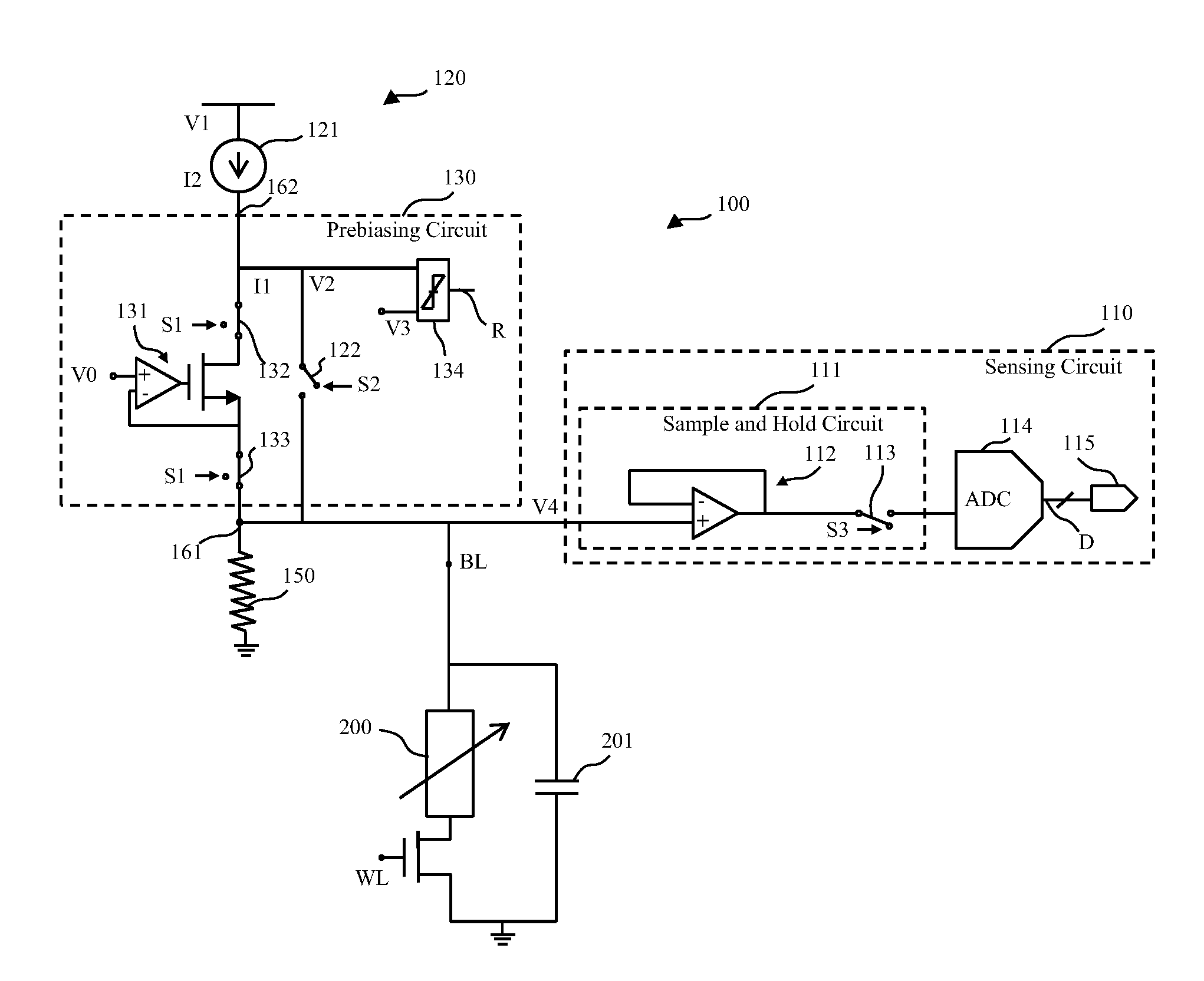
Figure 1 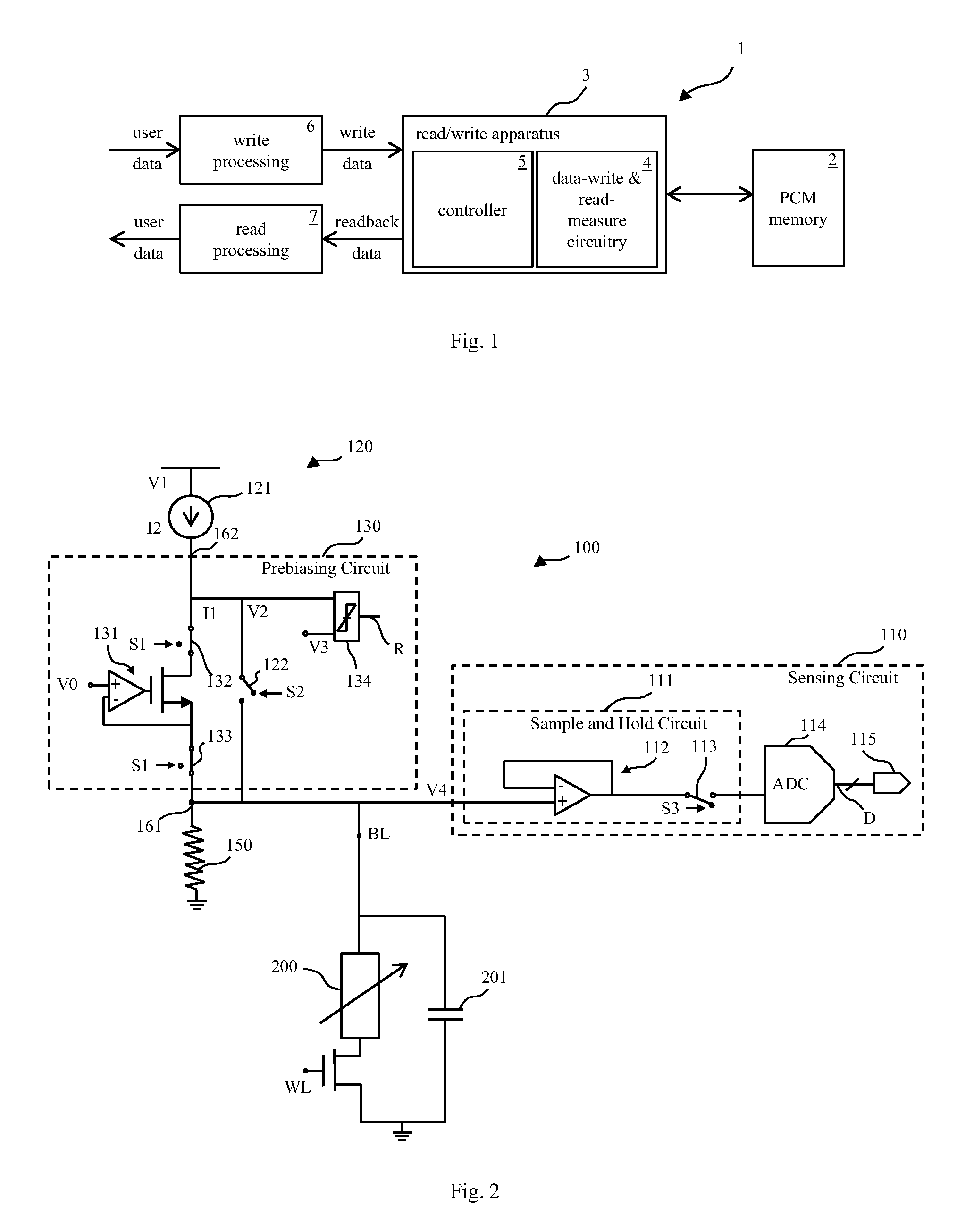
Figure 2 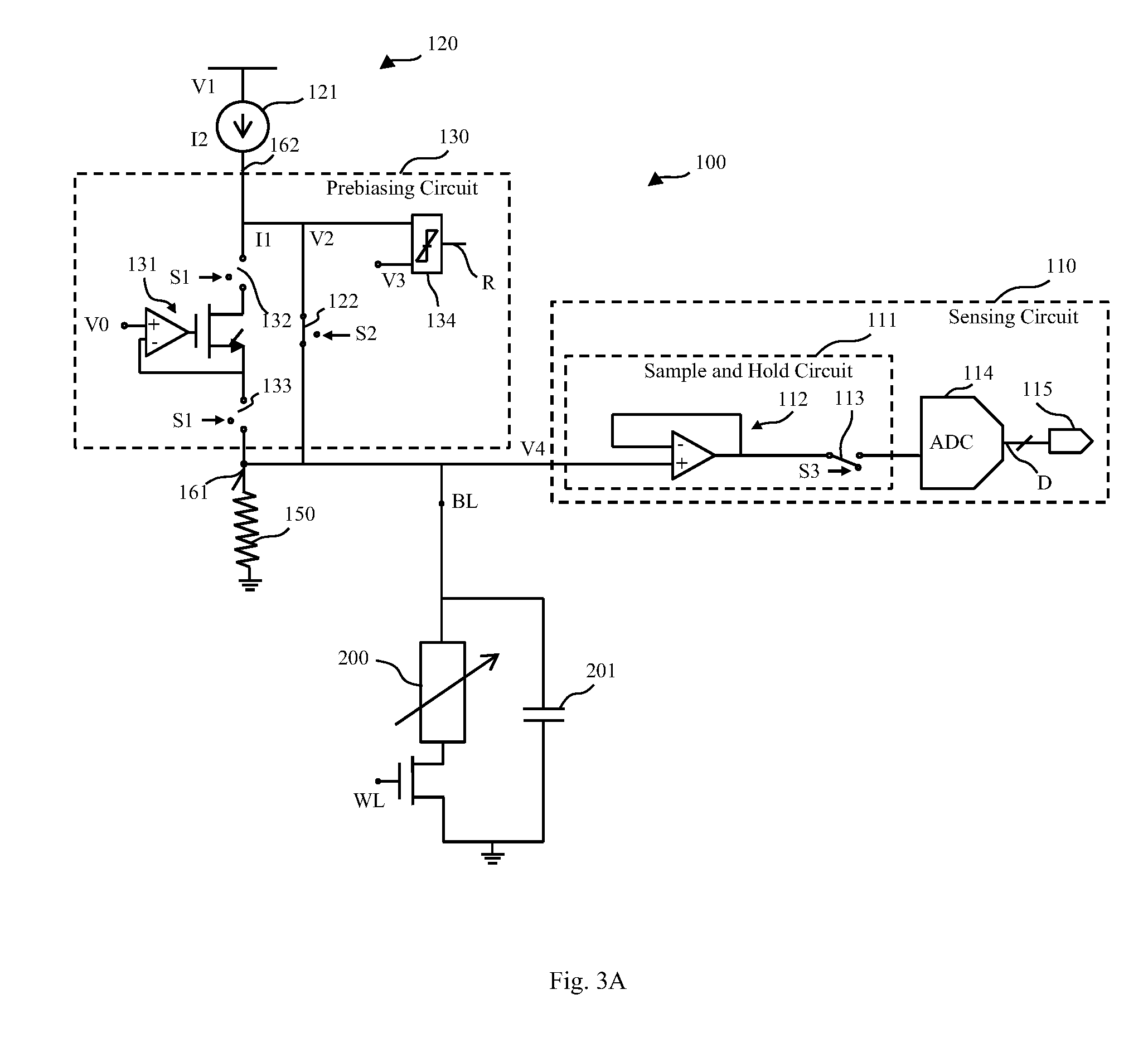
Figure 3
Abstract
Description
BACKGROUND
[0001] 1. Technical Field
[0002] The invention generally relates to a device and method for determining an actual cell state of a resistive memory cell having a plurality of programmable cell states.
[0003] 2. Description of the Related Art
[0004] A prominent example for resistive memory cells having a plurality of programmable levels or states is Resistive Random Access Memory (“RRAM”), in particular Phase Change Memory (“PCM”). PCM is a non-volatile solid-state memory technology that exploits the reversible, thermally-assisted switching of specific chalcogenides between certain states of different electrical conductivity.
[0005] PCM is a promising and advanced emerging non-volatile memory technology mainly due to its excellent features including low latency, high endurance, long retention and high scalability. PCM may be considered a prime candidate for Flash replacement, embedded / hybrid memory and storage-class memory. Key requirements for competitiveness of PCM technology may b...
Examples
first embodiment
[0065]In FIG. 2, a device 100 for determining an actual cell state of a resistive memory cell 200 in a prebiasing mode is depicted.
[0066]The device 100 of FIG. 2 has a sensing circuit 110, a settling circuit 120, a prebiasing circuit 130 and a resistor 150. The resistor 150 is coupled in parallel to the resistive memory cell 200. For example, the resistive memory cell 200 is a PCM cell having a plurality M of programmable cell states.
[0067]The sensing circuit 110 is configured to sense a sensing voltage V4 of the resistive memory cell 200 and to output a resultant value D (e.g., a digital value D) in response to the sensing voltage V4. The sensing voltage V4, and therefore also the resultant value D, are indicative for the actual cell state.
[0068]The sensing circuit 110 includes a sample and hold circuit 111, an analog-to-digital converter (“ADC”) 114 and an output 115. The sample and hold circuit 111 includes a buffer 112 and a switch 113 controlled by control signal S3.
[0069]The s...
second embodiment
[0083]Further, FIGS. 5-7 show the device 100 in different operating modes.
[0084]FIG. 5 shows the device 100 in the prebiasing mode. In the prebiasing mode, the switch 122 is opened, the switch 143 is closed and the switch 113 is opened. In FIG. 5, the current flows from the voltage source 141 over the first node 161 to the bitline BL and therefore to the resistive memory cell 200. The current flow in FIG. 5 is shown by arrow A1.
[0085]Further, in the settling mode according to FIG. 6, the switch 143 is opened, the switch 122 is closed and the switch 113 is open. As a result, the current flows from the current mirror 121 to the resistive memory cell 200 over the first node 161 and the bitline BL. The current flow in FIG. 6 is shown by arrow A2.
[0086]In FIG. 7, the device 100 is in a sampling mode. In the sampling mode, the switch 143 is opened, the switch 122 is closed and the switch 113 is closed. The controller controls the sampling by the third control signal S3 applied to switch 1...