

Method of manufacturing display substrate, repair method of display substrate and display substrate repaired by the repair method
a technology of display substrate and repair method, which is applied in the direction of static indicating devices, semiconductor/solid-state device testing/measurement, instruments, etc., can solve the problems of increased possibility of failure for repair, deterioration of display quality of lcd panel, and failure of signal line of array substrate, so as to reduce the height of the repair hole rh1, prevent foreign material defect of line, and reduce the effect of display substrate damag
Patent Information
- Authority / Receiving Office
- US · United States
- Current Assignee / Owner
- Publication Date
- 2016-05-19
Smart Images
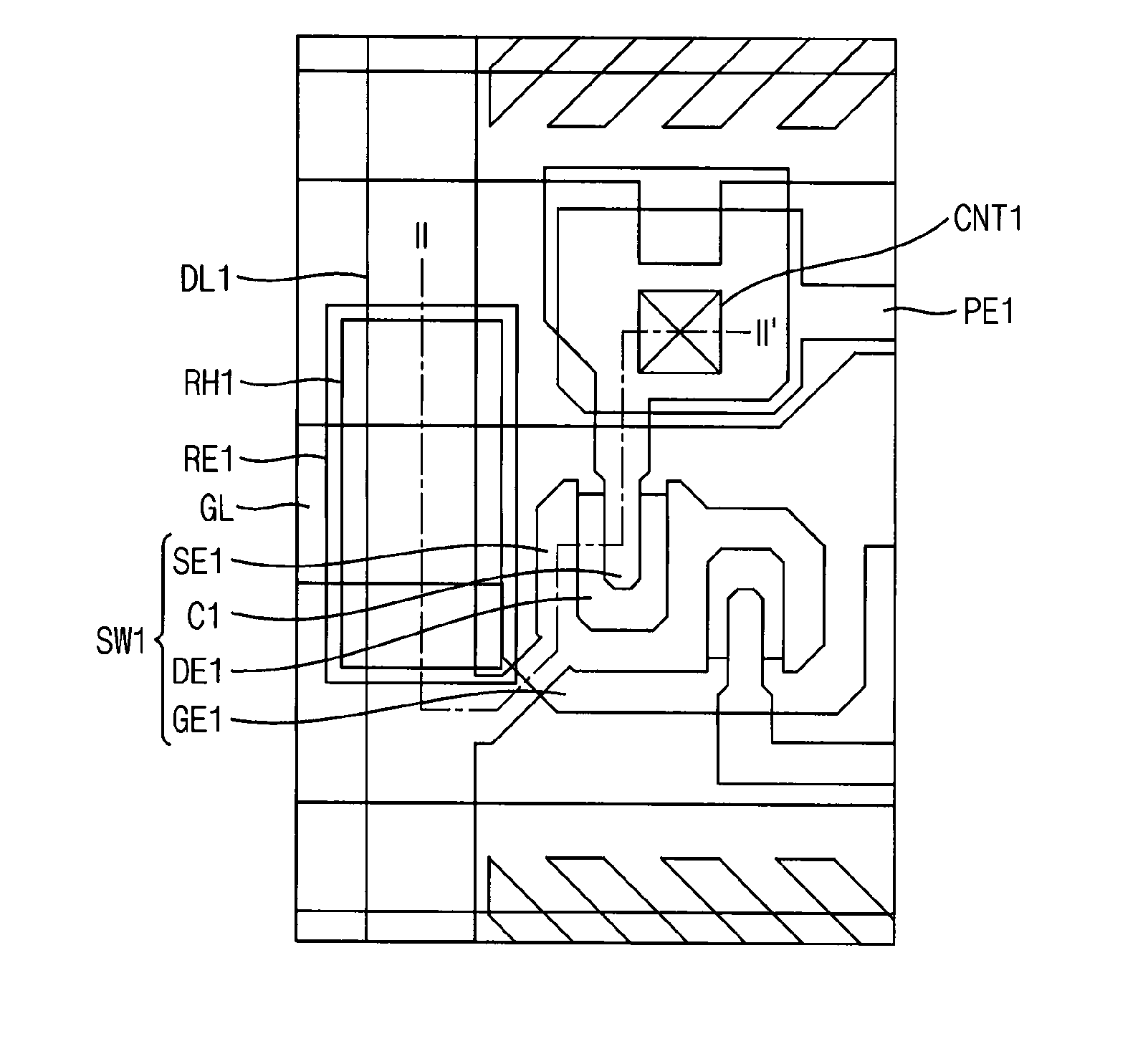
Figure 1 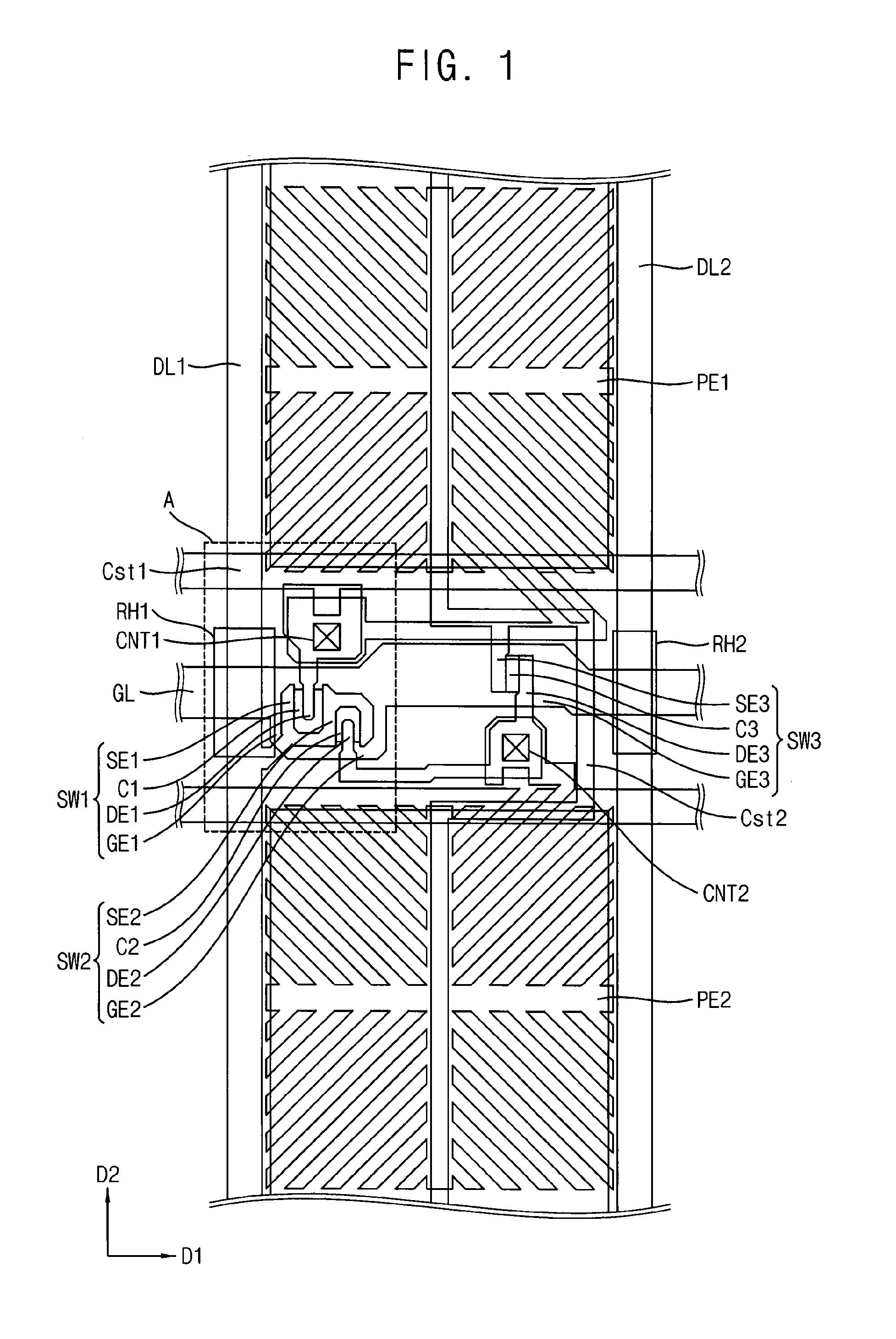
Figure 2 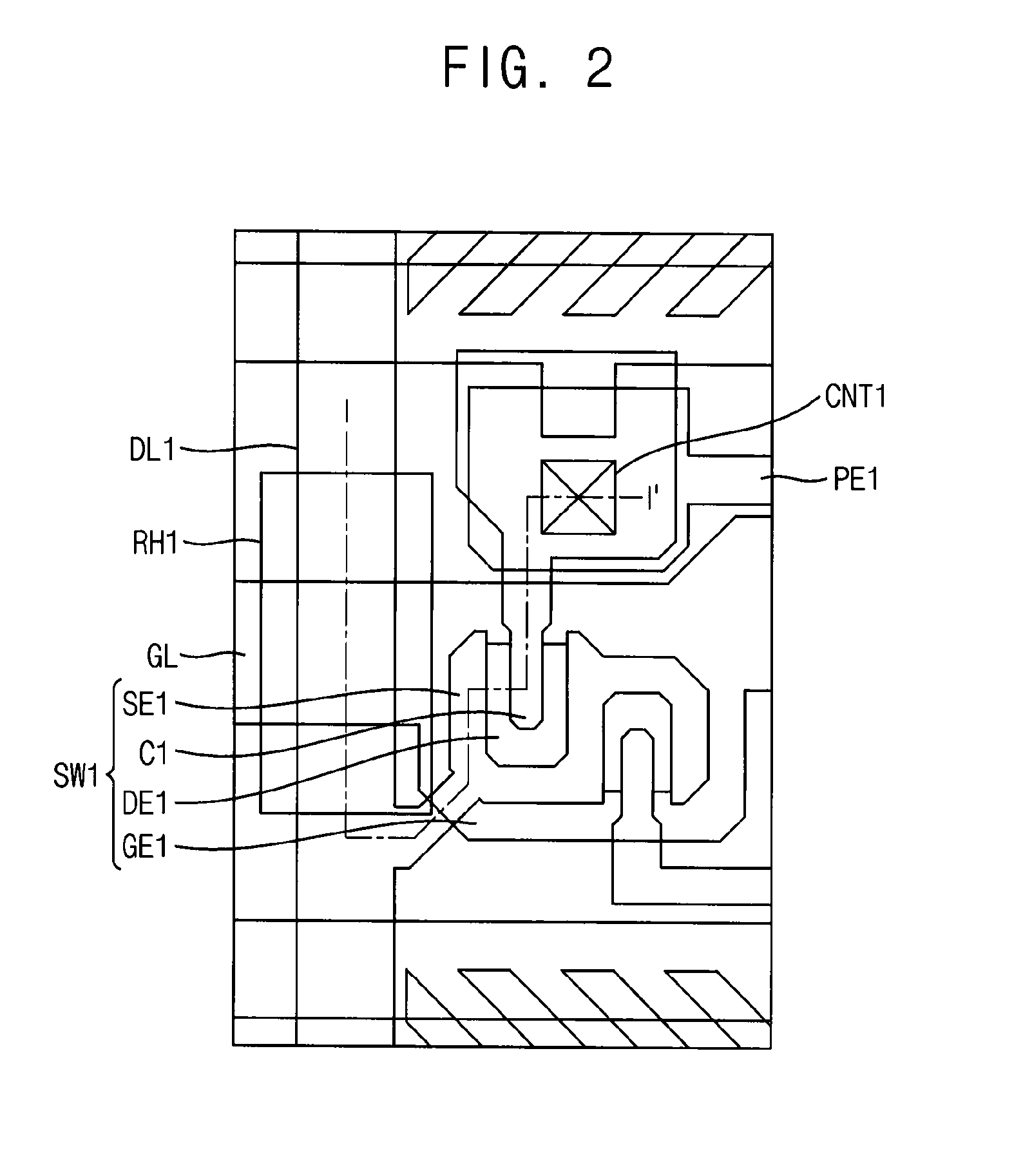
Figure 3
Abstract
Description
CLAIM OF PRIORITY
[0001] This application claims the priority of and all the benefits accruing under 35 U.S.C. §119 to Korean Patent Application No. 10-2014-0160797, filed on Nov. 18, 2014 in the Korean Intellectual Property Office (“KIPO”), the contents of which are herein incorporated by reference in their entireties.BACKGROUND OF THE INVENTION
[0002] 1. Field of the Invention
[0003] Exemplary embodiments of the present inventive concept relate to a method of manufacturing a display substrate, a method of repairing a display substrate and a display substrate repaired by the method of repairing a display substrate.
[0004] 2. Description of the Related Art
[0005] Generally, a liquid crystal display (LCD) panel includes a thin film transistor (TFT) substrate, an opposing substrate and an LC layer. The TFT substrate includes a plurality of gate lines, a plurality of data lines crossing the gate lines, a plurality of TFTs connected with the gate lines and data lines, and a plurality of pixel ele...
Examples
Embodiment Construction
[0057]Hereinafter, the present invention will be explained in detail with reference to the accompanying drawings.
[0058]FIG. 1 is a plan view illustrating a display substrate according to an exemplary embodiment of the inventive concept. FIG. 2 is a plan view magnifying portion “A” of FIG. 1. FIG. 3 is a cross-sectional view taken along the line I-I′ of FIG. 2.
[0059]Referring to FIGS. 1 to 3, a display substrate includes a gate line GL, a first data line DL1, a second data line DL2, a first repair hole RH1, a second repair hole RH2, a first storage line Cst1, a second storage line Cst2, a first switching element SW1, a second switching element SW2, a third switching element SW3, a high-pixel electrode PE1 and a low-pixel electrode PE2.
[0060]The gate line GL extends in a first direction D1. The gate line GL may have a single layer structure including copper (Cu), silver (Ag), chrome (Cr), molybdenum (Mo), aluminum (Al), titanium (Ti), manganese (Mn) and a mixture thereof. In addition,...