
Method for manufacturing thin-film multilayer electronic component and thin-film multilayer electronic component
a multi-layer electronic component and multi-layer technology, applied in the direction of fixed capacitors, stacked capacitors, fixed capacitor details, etc., can solve the problems of difficult to reduce the size of monolithic ceramic capacitors and increase the capacitance, and achieve the effect of efficient and economical production
Patent Information
- Authority / Receiving Office
- US · United States
- Patent Type
- Patents(United States)
- Current Assignee / Owner
- Publication Date
- 2007-02-20
- Estimated Expiration
- Not applicable · inactive patent
Smart Images
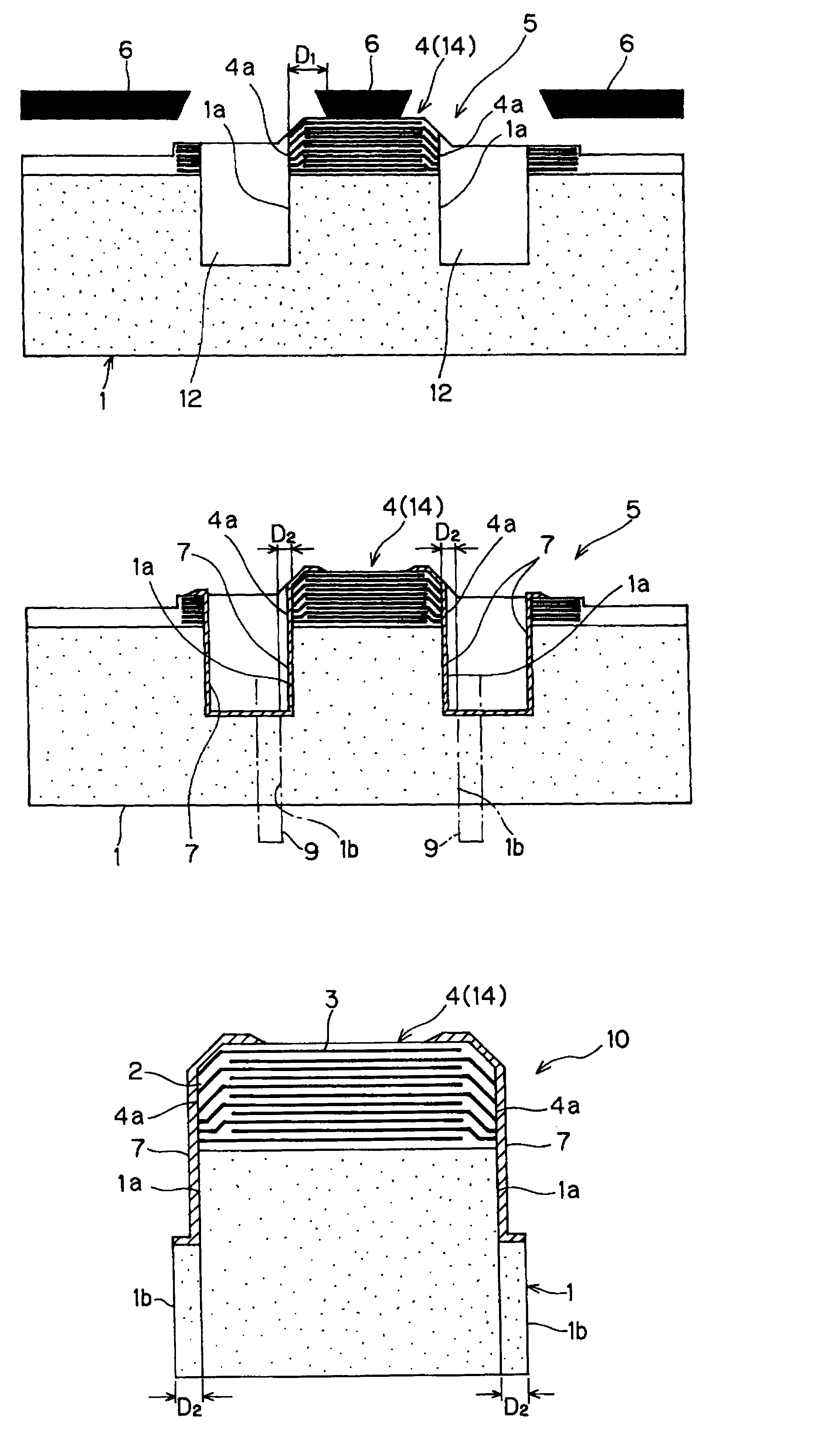
Figure 1 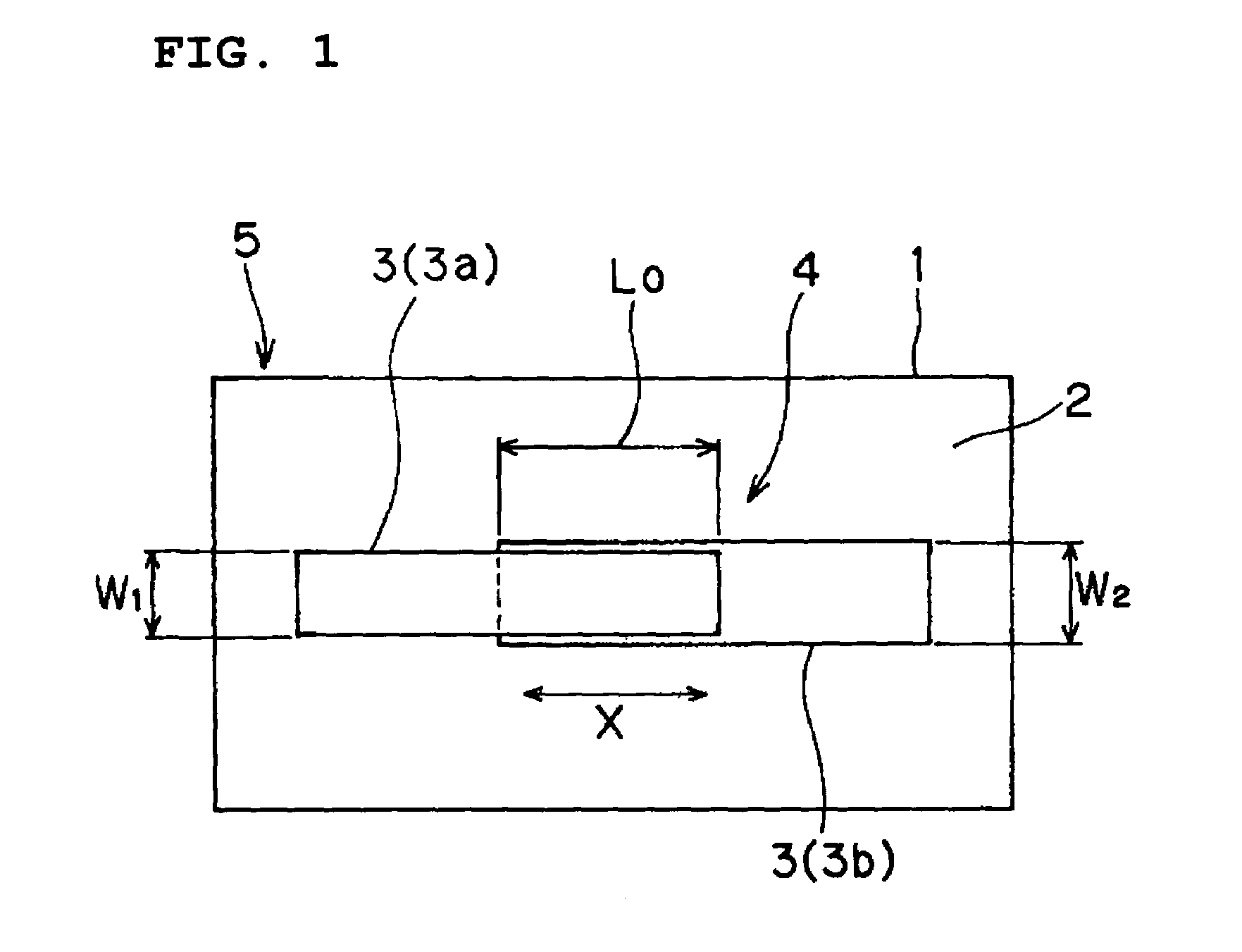
Figure 2 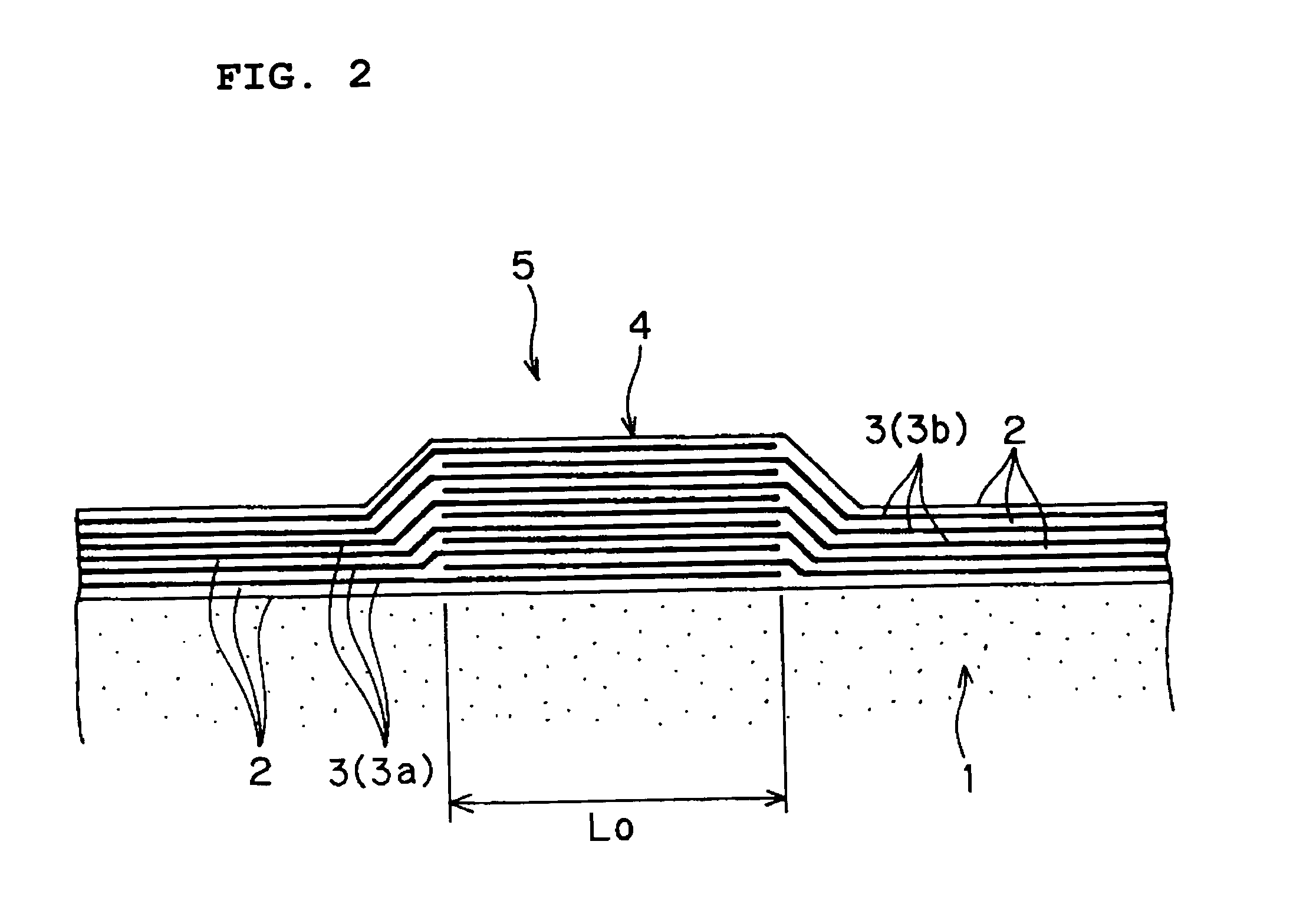
Figure 3
Abstract
Description
BACKGROUND OF THE INVENTION
[0001] 1. Field of the Invention
[0002] The present invention relates to multilayer electronic components, and more particularly, to a method for manufacturing a miniaturized thin-film multilayer electronic component, such as a thin-film multilayer capacitor, having a relatively high capacitance and further relates to such a thin-film multilayer electronic component.
[0003] 2. Description of the Related Art
[0004] A monolithic ceramic capacitor, which is typical of multilayer electronic components, is generally manufactured through the following steps:
[0005] (1) An electrode paste is printed on ceramic green sheets having a predetermined size.
[0006] (2) Then, a predetermined number of the ceramic green sheets are layered on one another, and ceramic green sheets not printed with the electrode paste are further layered on the upper and lower surfaces of the layered ceramic sheets, followed by contact-bonding under predetermined conditions to prepare a laminate.
[0007] ...
Examples
Embodiment Construction
[0042]The present invention will further be illustrated in detail with reference to preferred embodiments thereof.
[0043]Preferred embodiments will be described using a thin-film multilayer capacitor as the thin-film multilayer electronic component.
[0044]FIG. 1 is a transparent plan view of a laminate according to a preferred embodiment, prepared by layering dielectric thin films and thin-film internal electrodes on a substrate; FIG. 2 is a front sectional view of main portions of the laminate; FIG. 3 is a plan view of a laminated structure including the substrate and the laminate, having grooves; and FIG. 4 is a front sectional view of the structure shown in FIG. 3.
[0045](1) Dielectric thin films 2 and thin-film internal electrodes 3 are alternately deposited on a sapphire substrate 1 having a thickness of about 0.2 mm, as shown in FIG. 1, to prepare a laminate 4 (see FIG. 2). In this instance, the thin-film internal electrodes 3 are alternately displaced in a predetermined directio...