
Method to build robust mechanical structures on substrate surfaces
a technology of mechanical structure and substrate surface, which is applied in the direction of photomechanical apparatus, instruments, and semiconductor/solid-state device details, etc., can solve the problems of unable to manufacture robust parts, catastrophic failure of the connection of the seed layer to the substrate surface, and more likely to occur peeling or breaking of the metal seed layer from the substrate, etc., to achieve the effect of robust mechanical structur
Patent Information
- Authority / Receiving Office
- US · United States
- Patent Type
- Patents(United States)
- Current Assignee / Owner
- Publication Date
- 2007-08-07
- Estimated Expiration
- Not applicable · inactive patent
Smart Images

Figure 1 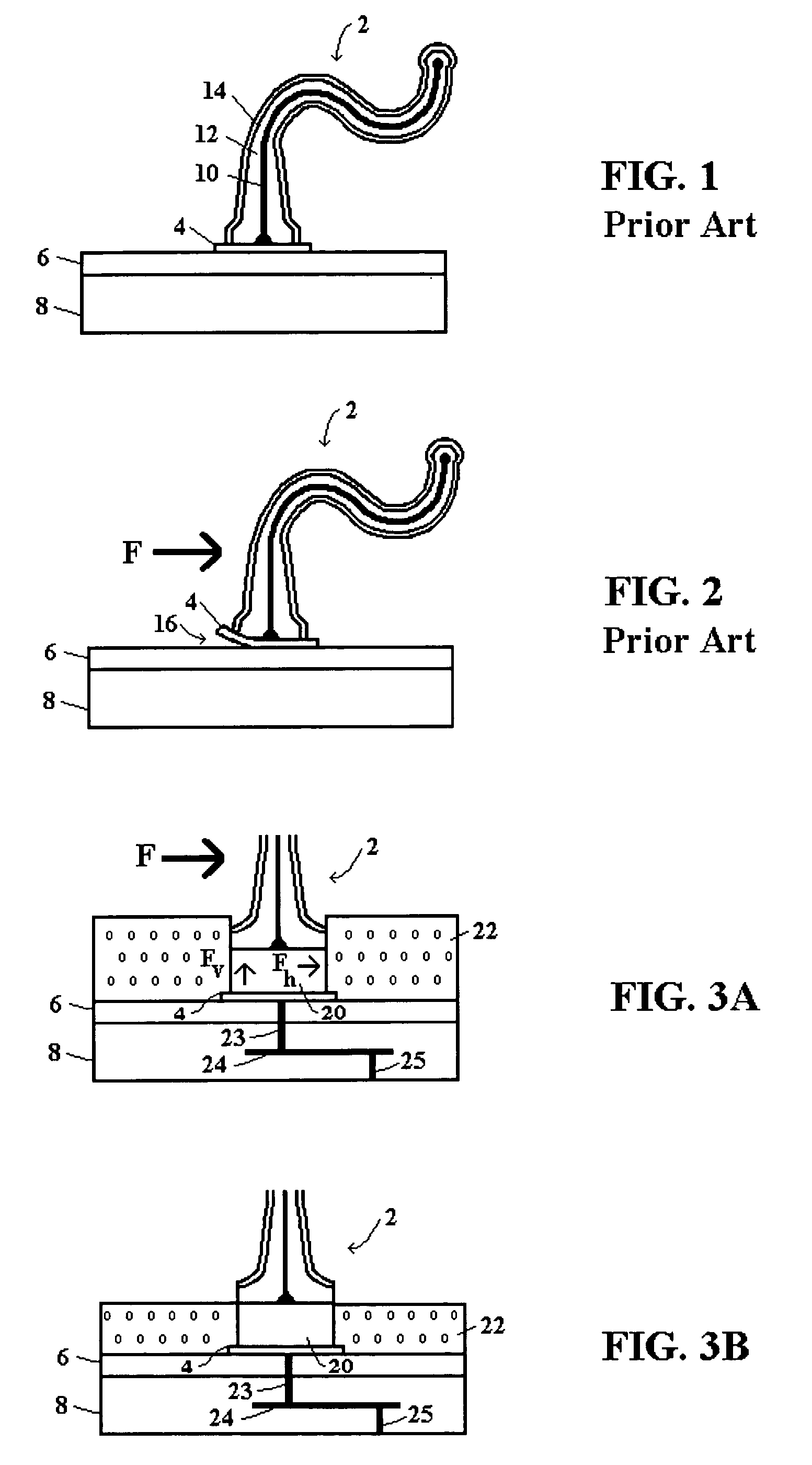
Figure 2 
Figure 3
Abstract
Description
BACKGROUND
[0001] 1. Technical Field
[0002] The present invention relates in general to fabrication of a mechanical structure on a substrate surface for robustly mounting Micro Electro Mechanical Systems (MEMS). More particularly, the present invention relates to a structure provided on a substrate surface for robustly mounting spring probes used on probe cards for testing integrated circuits on wafers.
[0003] 2. Related Art
[0004] Mechanical structures are fabricated on substrate surfaces for a variety of applications. The substrate surfaces include polymers, metals, ceramics, semiconductors, etc. Typically to make electrical contact, a metal seed layer is deposited on the substrate surface to form bond pads for mounting the mechanical structures. As the size of the bond pad shrinks to accommodate smaller structures such as MEMS, or to accommodate limited spacing between small structures in an array, peeling or breaking of the metal seed layer from the substrate is more likely to occur, pa...
Examples
Embodiment Construction
[0032]FIG. 3A illustrates a robust mechanical structure for supporting spring probes according to the present invention, including a foundation formed over a bond pad 4 for supporting a spring probe 2, a reinforcing insulation layer 22 provided around the foundation, and application of a force F to a spring probe 2 formed on the foundation. FIG. 3A includes a substrate 8 with a insulation coating layer 6 and a metal seed layer bond pad 4 formed on the layer 6, as described in FIGS. 1-2. In FIG. 3A, components carried over from FIGS. 1 and 2 are similarly labeled, as will be components carried over in subsequent drawings.
[0033]To provide the foundation, FIG. 3A includes a metal plating layer 20 applied over the metal seed layer 4. The spring probe 2 is shown constructed on the metal plating layer 20. A dielectric material 22 is provided over the exposed polymer surface 6, around the edges of the metal seed layer pad 4, around the edges of the metal plating layer 20, on a portion of t...