
Method of fabricating SOI wafer
a technology of soi wafers and soi layers, which is applied in the direction of basic electric elements, electrical apparatus, semiconductor devices, etc., can solve the problems of increasing the risk of affecting the above-described method suffers from the drawbacks described, and the thickness distribution of the polished soi layer is more likely to worsen. , to achieve the effect of reducing the roughness of the separation surfa
Patent Information
- Authority / Receiving Office
- US · United States
- Patent Type
- Patents(United States)
- Current Assignee / Owner
- Publication Date
- 2008-01-22
- Estimated Expiration
- Not applicable · inactive patent
Smart Images
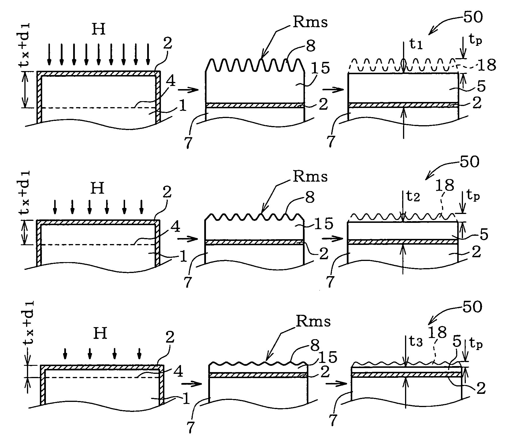
Figure 1 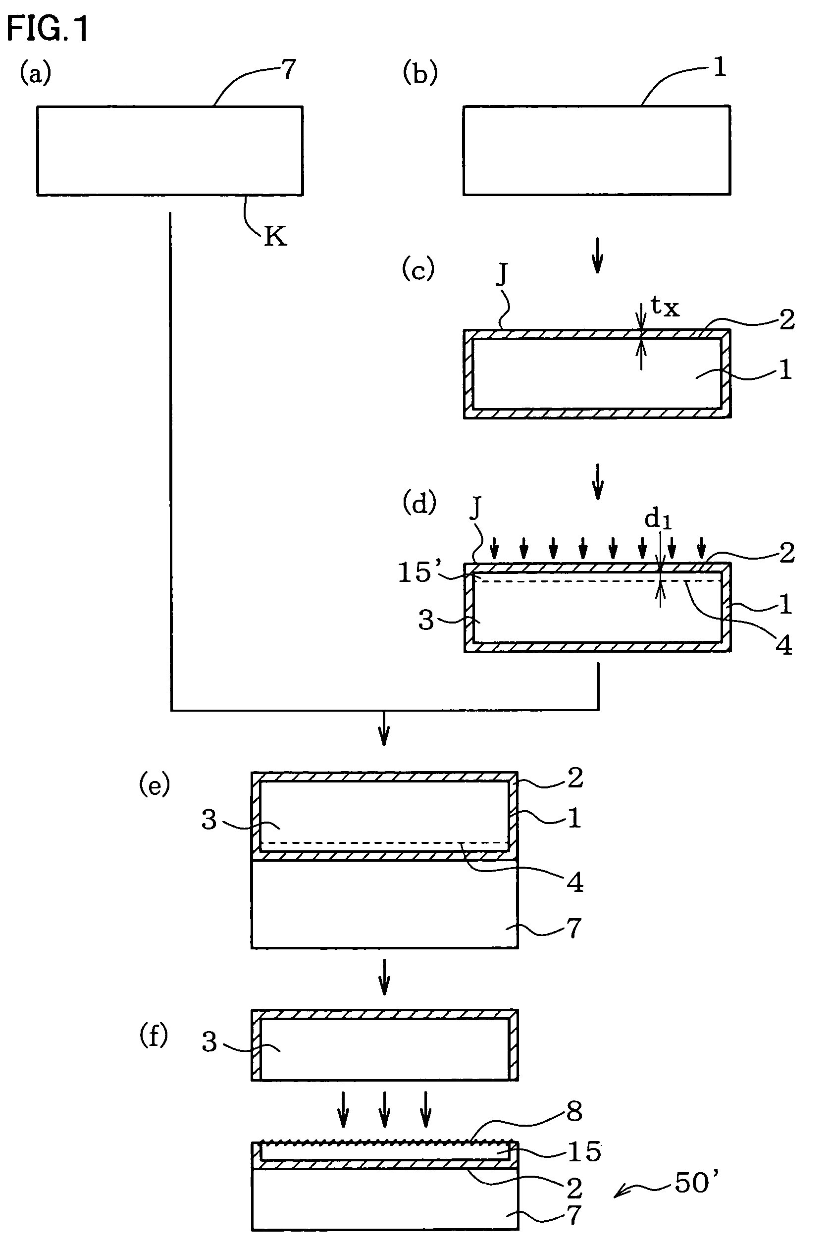
Figure 2 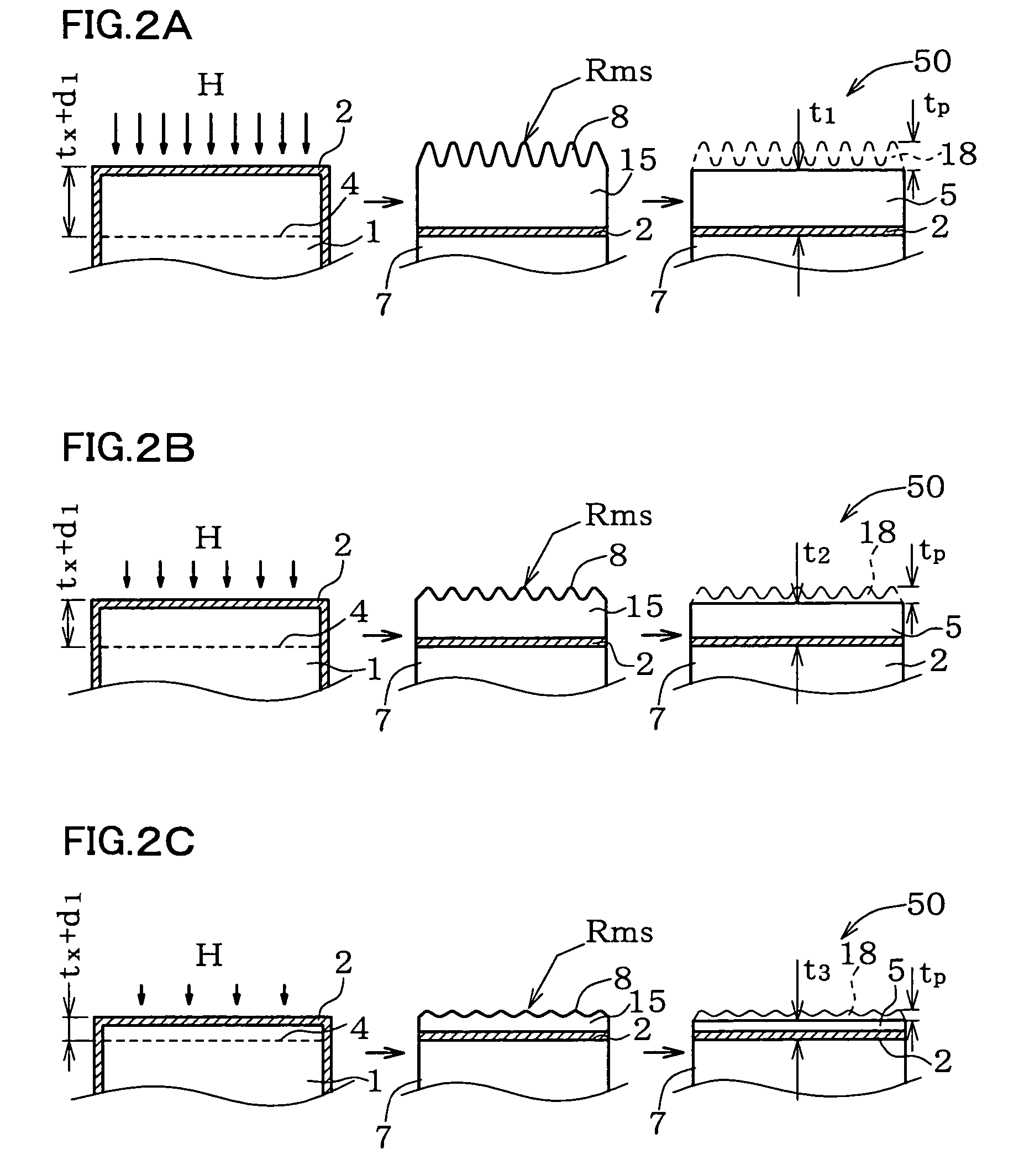
Figure 3
Abstract
Description
FIELD OF THE INVENTION
[0001] The present invention relates to a method of fabricating an SOI wafer.BACKGROUND ART
[0002] In the field of mobile communication using mobile phones or the like, it is becoming general to handle high frequency signals of several hundreds of megahertz, and this raises needs for semiconductor devices excellent in high-frequency characteristics. For example, semiconductor devices such as CMOS-IC and high-voltage-resistant-type IC adopt a so-called SOI wafer which is configured by forming a silicon oxide insulating layer (buried oxide film) on a silicon single crystal substrate (also referred to as “base wafer”, hereinafter), and by stacking thereon another silicon single crystal layer as an SOI (silicon on insulator) layer. For the case where the SOI wafer is applied to semiconductor devices for high-frequency use, it is necessary to use a silicon single crystal having a large resistivity as the base wafer, in view of suppressing high-frequency loss.
[0003] Bond...
Examples
Embodiment Construction
[0027]The following paragraphs will describe best modes for carrying out the invention.
[0028]FIG. 1 is a drawing explaining a basic embodiment of the method of fabricating an SOI wafer according to the present invention. First, a base wafer 7 shown in step (a) as a first substrate typically composed of silicon single crystal, and a bond wafer 1 shown in step (b) as a second silicon single crystal substrate are obtained. The bond wafer 1 has, as shown in step (c), a silicon oxide film 2 as an insulating film formed at least on a first main surface J side thereof. The silicon oxide film 2 can be formed by thermal oxidation such as wet oxidation or dry oxidation, and it is also allowable to adopt a method such as CVD (chemical vapor deposition). Thickness of the silicon oxide film tx is adjusted to approximately 50 nm to 2 μm, both ends inclusive, considering that it is used as an insulating layer typically for MOS-FET. The base wafer 7 may be an insulating substrate such as quartz sub...