
FET bias circuit
a field effect transistor and bias circuit technology, applied in the direction of amplifiers, amplifiers with semiconductor devices only, amplifiers, etc., can solve the problems of loss of power applied to the fet, the inability to work with large fet devices where high efficiency is required, etc., to reduce the variation of gain and linear characteristics due to static drain current, the effect of reducing the size and power consumption of the circui
Patent Information
- Authority / Receiving Office
- US · United States
- Patent Type
- Patents(United States)
- Current Assignee / Owner
- Publication Date
- 2008-09-02
- Estimated Expiration
- Not applicable · inactive patent
Smart Images
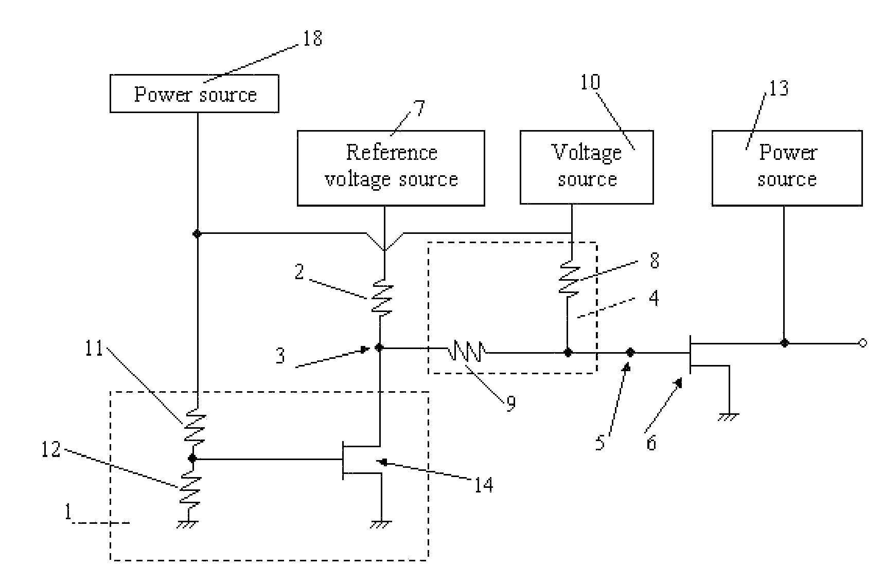
Figure 1 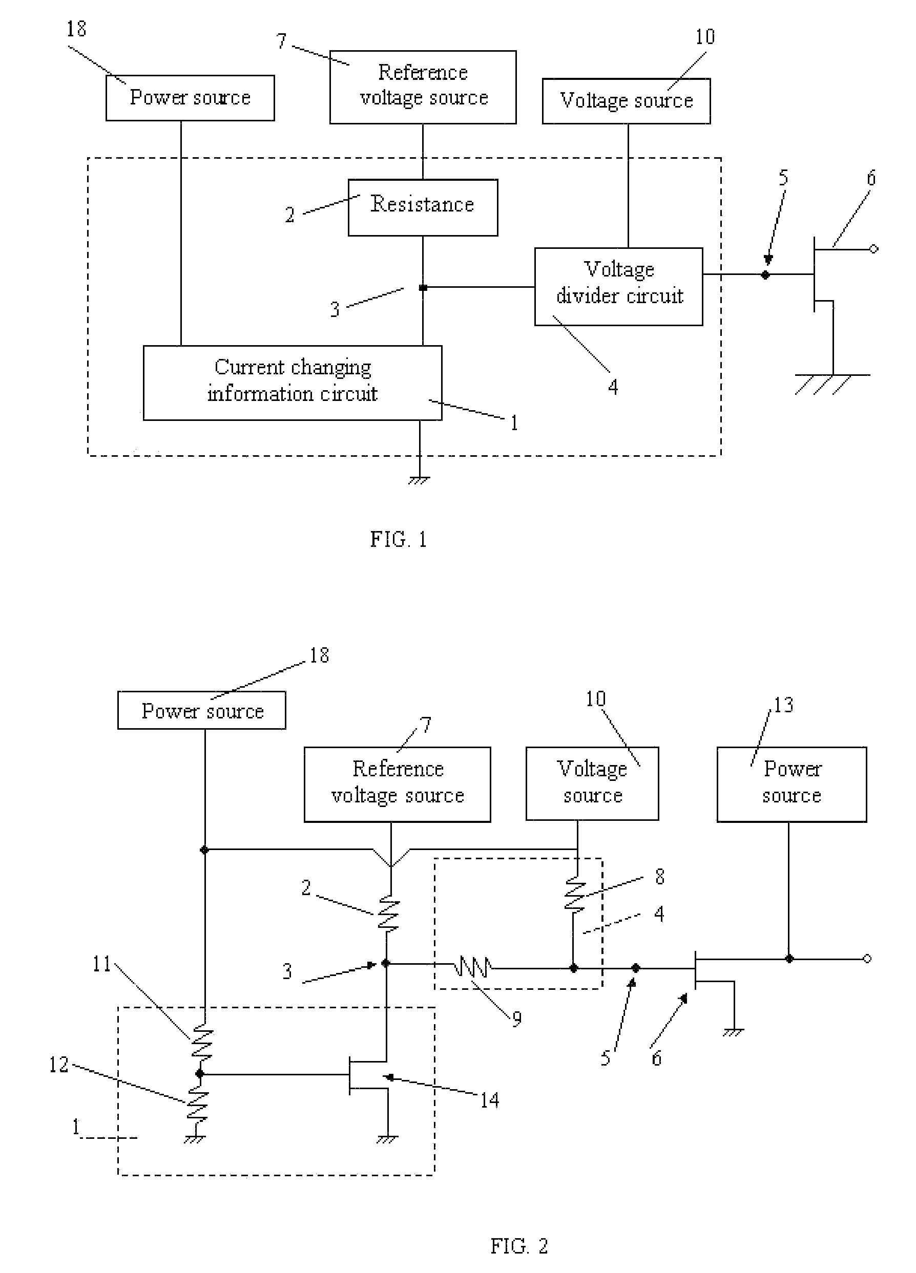
Figure 2 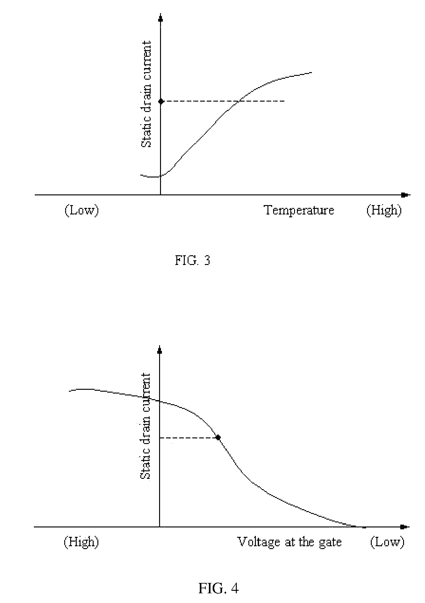
Figure 3
Abstract
Description
CROSS-REFERENCE TO RELATED APPLICATIONS
[0001] This is a National Stage Application of International Patent Application No. PCT / CN 2005 / 000516 with an international filing date of Apr. 18, 2005, which is based on Chinese Patent Application No. 200410056160.4, filed Aug. 2, 2004. The contents of both of these specifications are incorporated herein by reference.BACKGROUND OF THE INVENTION
[0002] 1. Field of the Invention
[0003] This invention relates to an FET (Field Effect Transistor) bias circuit, and specifically to a highly-efficient FET bias circuit capable of overcoming static drain current variations of an FET due to temperature variations, lowering the variations of the gain and the linear characteristics of an FET due to temperature variations, as well as reducing the distributional variations of the static gain current of FETs manufactured at different portions of a silicon wafer.
[0004] 2. Description of the Related Art
[0005] When designing a circuit comprising an FET (Field Effect ...
Examples
first embodiment
[0025]FIG. 2 shows an FET bias circuit of a first embodiment in accordance with the present invention. In the present embodiment, a current changing information circuit 1 comprises an FET 14 and two voltage divider resistors 11, 12 connected in series; wherein, the source of the FET 14 is grounded; the drain is connected to a reference voltage source 7 by means of a resistor 2; the gate is connected to a position between the resistor 11 and the resistor 12; one end of the resistor series11, 12 is grounded, the other end is connected to a power source 18, which is sharing the same supply with the voltage source 10, and which is applied to the gate of the FET 14 via voltage divider resistors 11, 12, thereby setting the static drain current of the FET 14. The node between the current-changing information circuit 1 and the resistor 2 acts as an output end 3 providing voltage-changing information is connected to a voltage divider circuit 4 having two resistors 8, 9 connected in series; w...
second embodiment
[0042]FIG. 9 shows an FET bias circuit of the present invention, illustrating a similar circuit configuration to that shown in FIG. 2, except that the current-changing information circuit 1 comprises a diode. One end of the diode is grounded, the other end of the diode is connected to one end of a resistor 2, the other end of the resistor 2 is connected to a reference voltage source 7, and the node between the resistor 2 and the diode acts as an output end 3 providing the voltage-changing information. Since the current-changing characteristics of a diode are similar to those of the FET, the function of the present invention can also be realized by associating a diode with the setting of the voltage divider circuit 4. Here, it is not necessary to use the power source 18, and it can be kept in an open state.
third embodiment
[0043]FIG. 10 shows an FET bias circuit of the present invention, illustrating a similar circuit configuration to that shown in FIG. 2, except that the power source 18 is a separate one.
[0044]FIG. 11 is based on the circuit shown in FIG. 10 and illustrates the adjustment of the static drain current of the FET 6 via an external micro-adjustment. The parts within the dashed line are integrated in the IC chip, while resistors 15, 16 shown outside the block are not necessarily so. When the static drain current of the FET 6 deviates from an ideal value due to variations in the process for IC chip fabrication, it can be micro-adjusted by the regulating resistors 15 and / or resistor 16 disposed outside the IC chip. In addition, the resistor 17 disposed inside the IC chip is applied to increase the isolation of components so as to avoid interference of signals from the current-changing information circuit 1 on the FET 6 when the value of the resistor 9 is small.
[0045]FIG. 12 shows a configur...