
Methods for oriented growth of nanowires on patterned substrates
a technology of nanowires and substrates, applied in the field of nanowires, can solve the problems of inconvenient mass production, current approaches to grow and harvest nanowires, etc., and achieve the effect of improving nanowire quality and reducing surface states
Patent Information
- Authority / Receiving Office
- US · United States
- Patent Type
- Patents(United States)
- Current Assignee / Owner
- Publication Date
- 2011-05-31
Smart Images
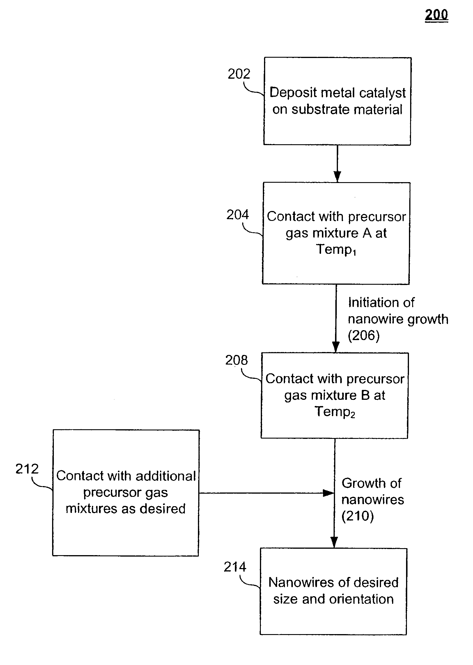
Figure 1 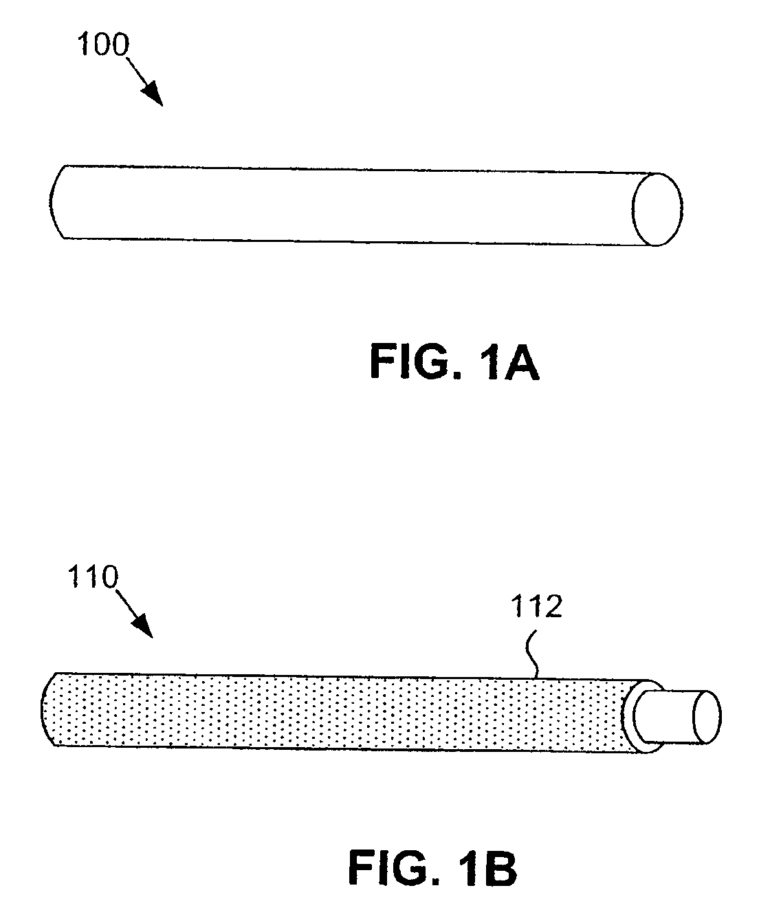
Figure 2 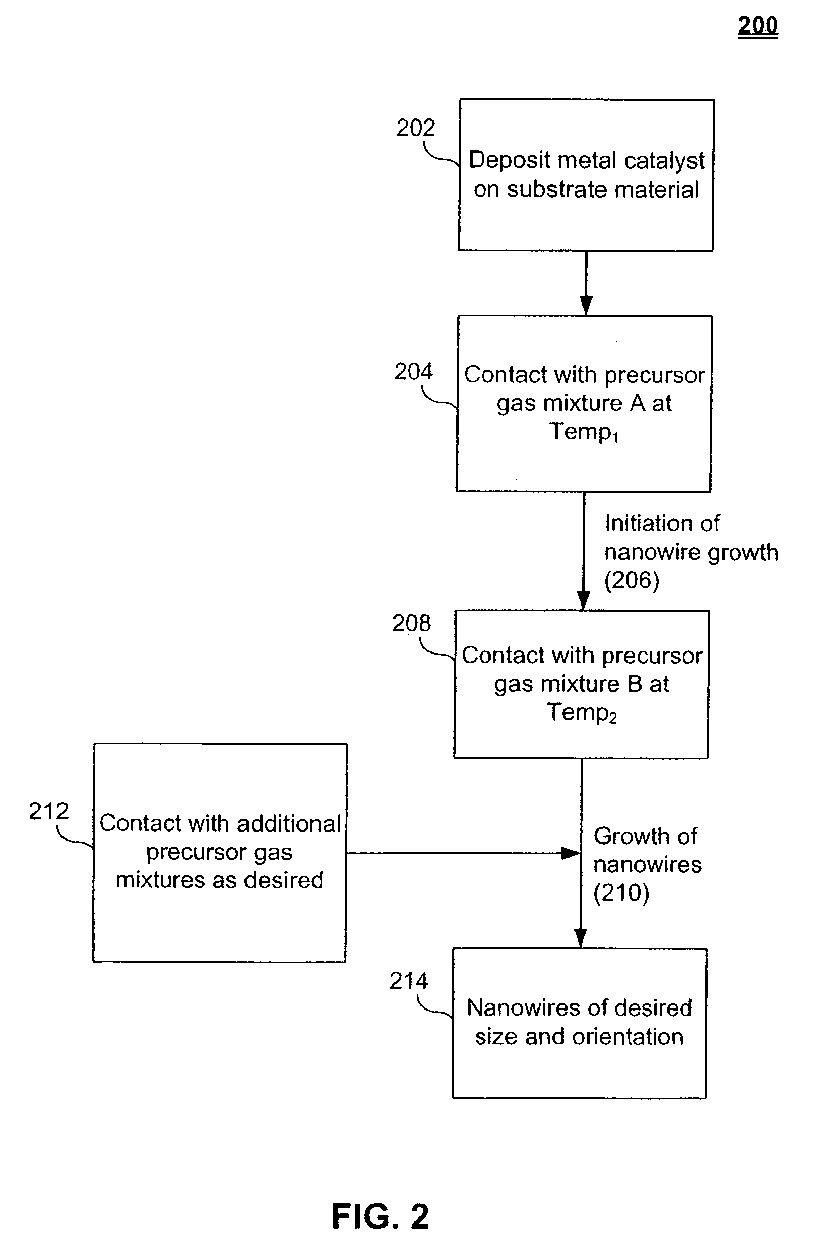
Figure 3
Abstract
Description
CROSS REFERENCE TO RELATED APPLICATIONS
[0001] This application claims the benefit of U.S. Provisional Patent Application No. 60 / 754,519, filed Dec. 29, 2005, the disclosure of which is incorporated herein by reference in its entirety.BACKGROUND OF THE INVENTION
[0002] 1. Field of the Invention
[0003] The present invention relates to nanowires, and more particularly, to nanowire growth and harvesting.
[0004] 2. Background of the Invention
[0005] Nanostructures, and in particular, nanowires have the potential to facilitate a whole new generation of electronic devices. A major impediment to the emergence of this new generation of electronic devices based on nanostructures is the ability to effectively grow and harvest nanowires and other nanostructures that have consistent characteristics. Current approaches to grow and harvest nanowires do not facilitate mass production and do not yield consistent nanowire performance characteristics.
[0006] What are needed are systems and methods to grow and ha...
Examples
Embodiment Construction
[0055]It should be appreciated that the particular implementations shown and described herein are examples of the invention and are not intended to otherwise limit the scope of the present invention in any way. Indeed, for the sake of brevity, conventional electronics, manufacturing, semiconductor devices, and nanowire (NW), nanorod, nanotube, and nanoribbon technologies and other functional aspects of the systems (and components of the individual operating components of the systems) may not be described in detail herein. Furthermore, for purposes of brevity, the invention is frequently described herein as pertaining to nanowires.
[0056]It should be appreciated that although nanowires are frequently referred to, the techniques described herein are also applicable to other nanostructures, such as nanorods, nanotubes, nanotetrapods, nanoribbons and / or combinations thereof. It should further be appreciated that the manufacturing techniques described herein could be used to create any se...