
Electron emission device
Patent Information
- Authority / Receiving Office
- US · United States
- Current Assignee / Owner
- Publication Date
- 2005-09-01
- Estimated Expiration
- Not applicable · inactive patent
Smart Images
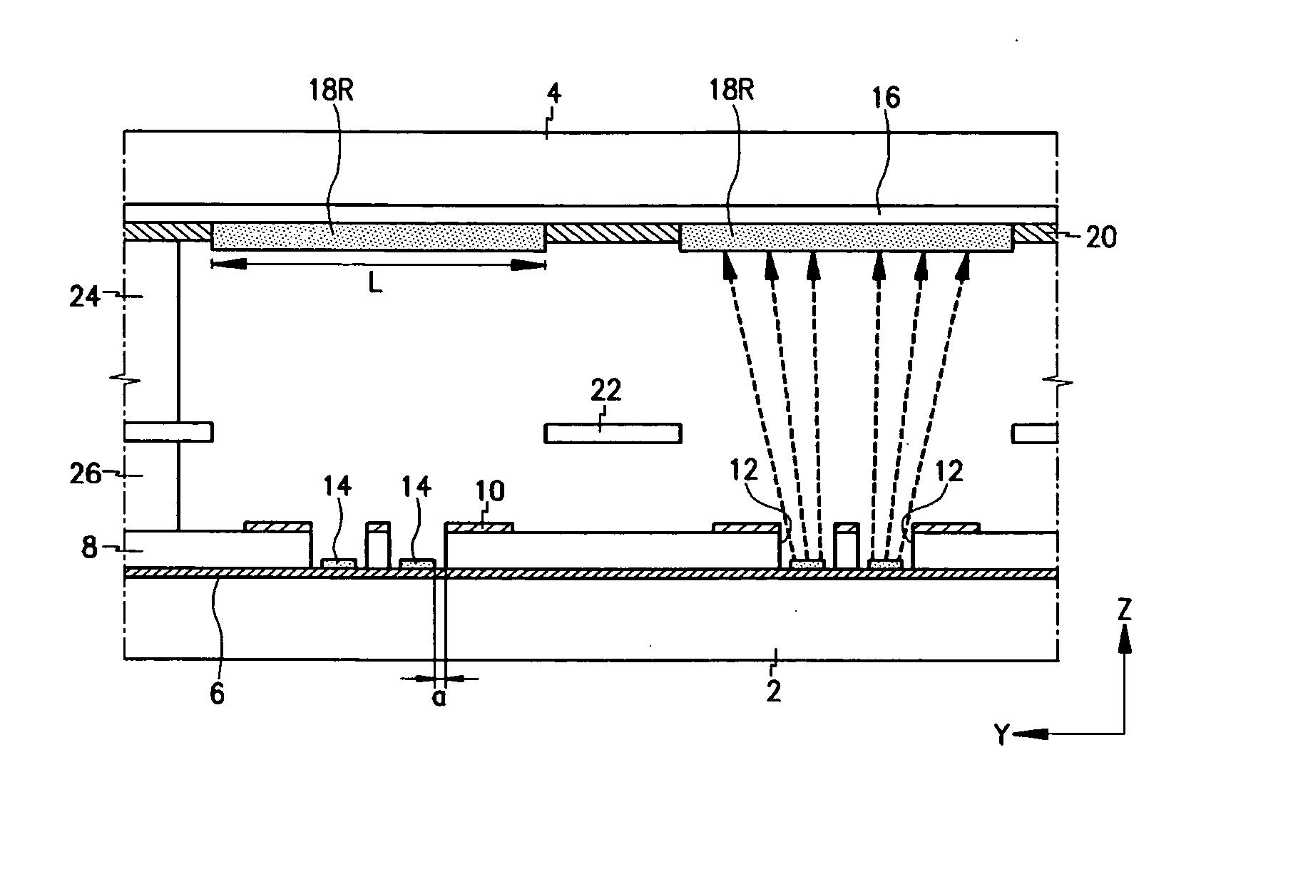
Figure 1 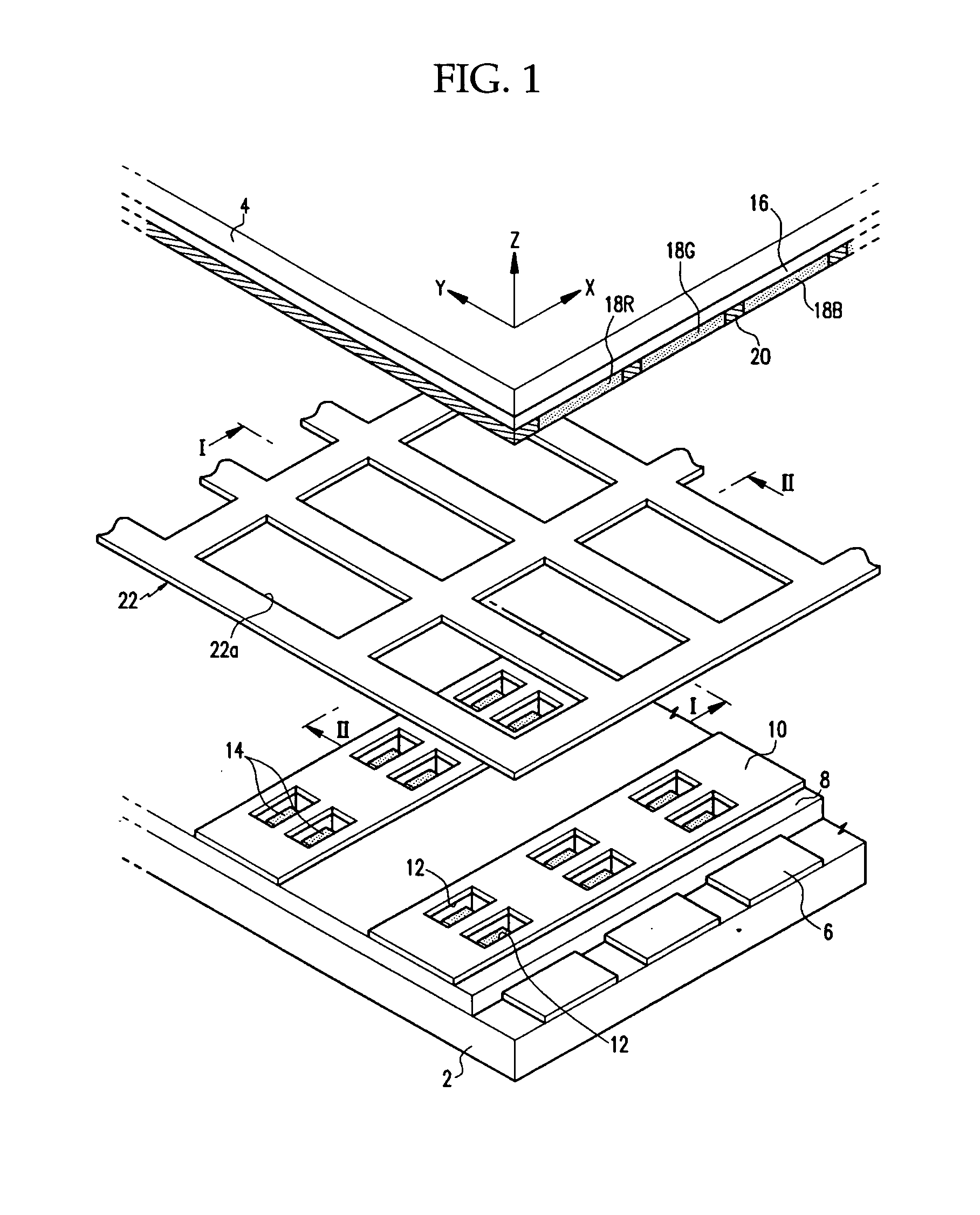
Figure 2 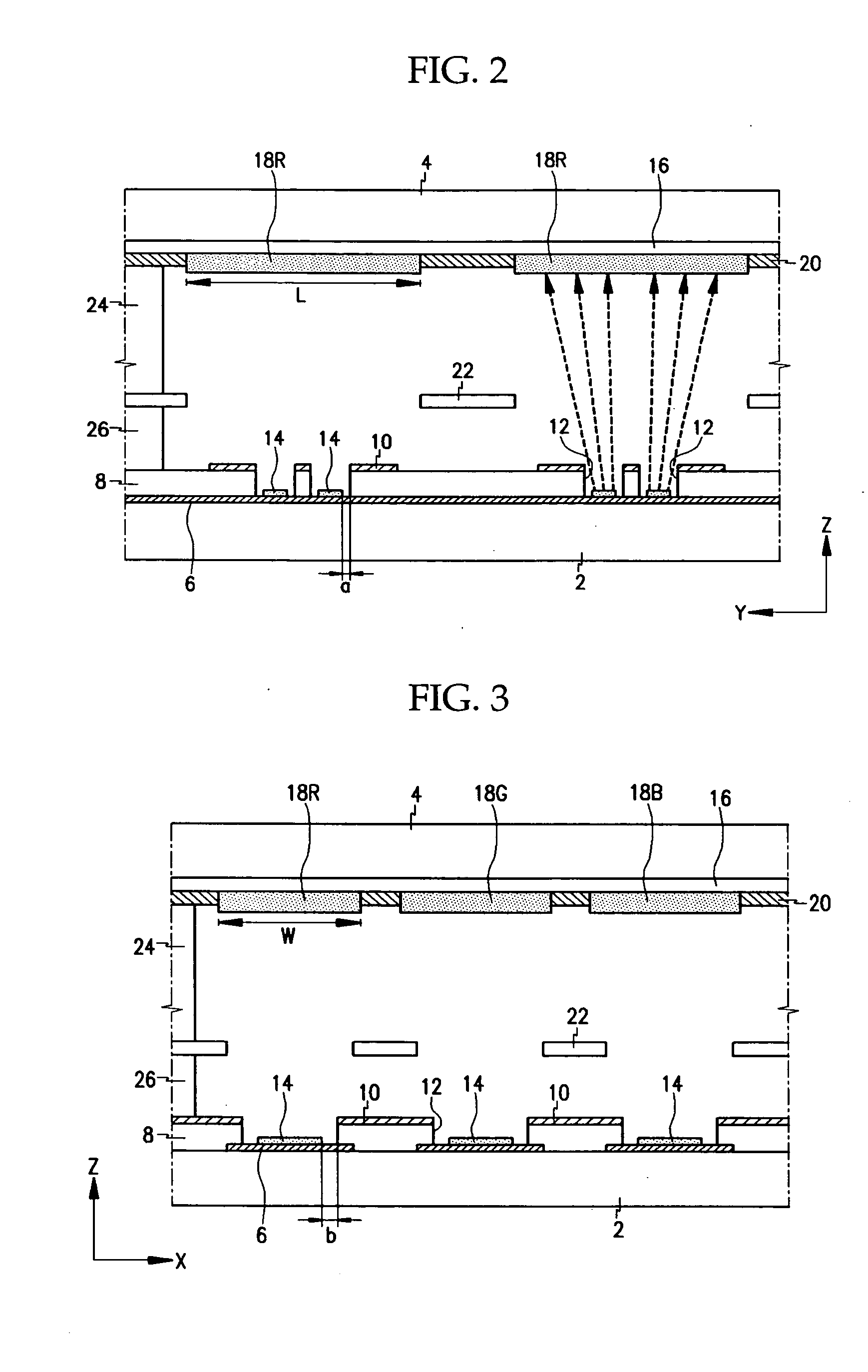
Figure 3
Abstract
Description
CROSS REFERENCE TO RELATED APPLICATION
[0001] This application claims priority to and the benefit of Korea Patent Application No. 2004-0012951 filed on Feb. 26, 2004 in the Korean Intellectual Property Office, the content of which is incorporated herein by reference. BACKGROUND OF THE INVENTION
[0002] (a) Field of the Invention
[0003] The present invention relates to an electron emission device, and in particular, to an electron emission device which has an electron emission source with an improved pattern to minimize the diffusion of electron beams, and enhance the screen color representation.
[0004] (b) Description of Related Art
[0005] Generally, the electron emission devices are classified into a first type where a hot cathode is used as an electron emission source, and a second type where a cold cathode is used as the electron emission source.
[0006] Among the second type electron emission devices there are field emitter array (FEA) types, surface conduction emitter (SCE) types...
Examples
Embodiment Construction
[0029] As shown in the FIGS. 1-3, wherein an FEA type is illustrated the electron emission device has first and second substrates 2, 4 sealed to each other at their peripheries by a sealant (not shown), such as frit, to form a vacuum vessel. A structure for emitting electrons upon formation of electric fields is provided at first substrate 2, and a structure of displaying the desired images due to light emission caused by the electrons is provided at second substrate 4.
[0030] Specifically, cathode electrodes 6 are formed on first substrate 2 in a stripe pattern while proceeding in a direction (in the Y direction of the drawing), and insulation layer 8 is formed on the entire inner surface of first substrate 2 while covering cathode electrodes 6. Gate electrodes 10 are formed on insulation layer 8 while proceeding in the direction crossing cathode electrodes 6 (in the X direction of the drawing), and openings 12 are formed at the respective crossed regions of the cathode and gate el...