
Deep trench varactors
a technology of deep trenches and varactors, applied in the field of deep trenches varactors, can solve the problems of corresponding increase in thickness, degradation of device performance, and negatively affecting the performance of such mos varactors, and achieve the effect of minimal leakage current and high areal capacitance density
Patent Information
- Authority / Receiving Office
- US · United States
- Patent Type
- Patents(United States)
- Current Assignee / Owner
- Publication Date
- 2011-08-30
- Estimated Expiration
- Not applicable · inactive patent
Smart Images
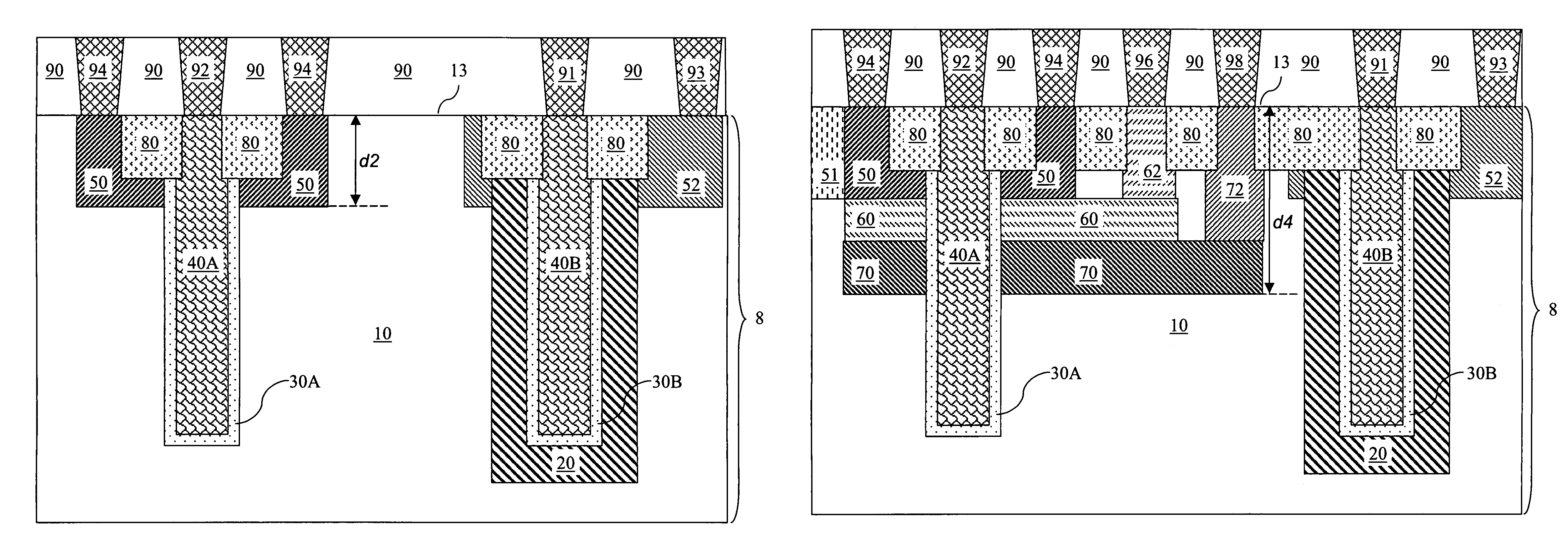
Figure 1 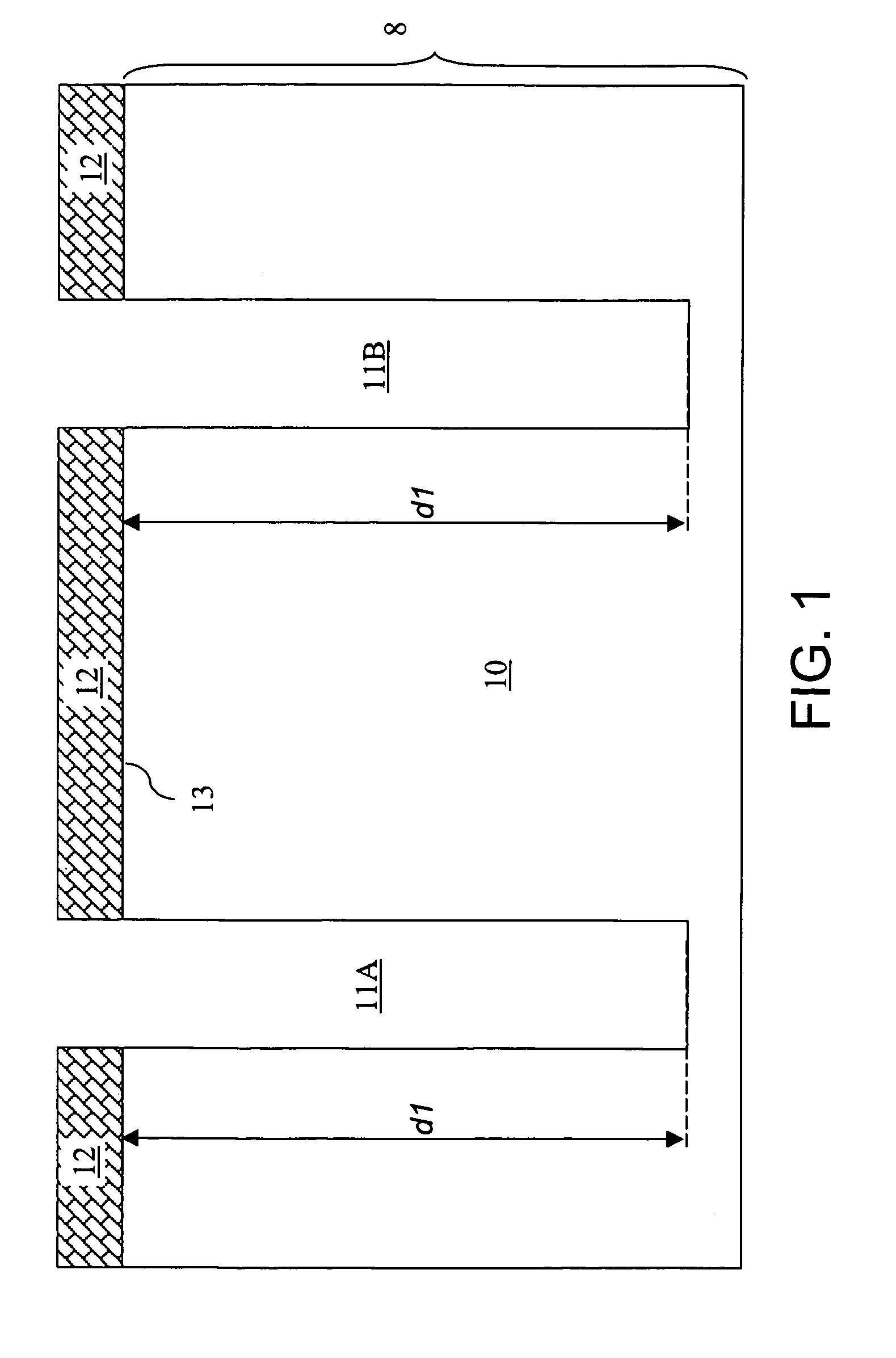
Figure 2 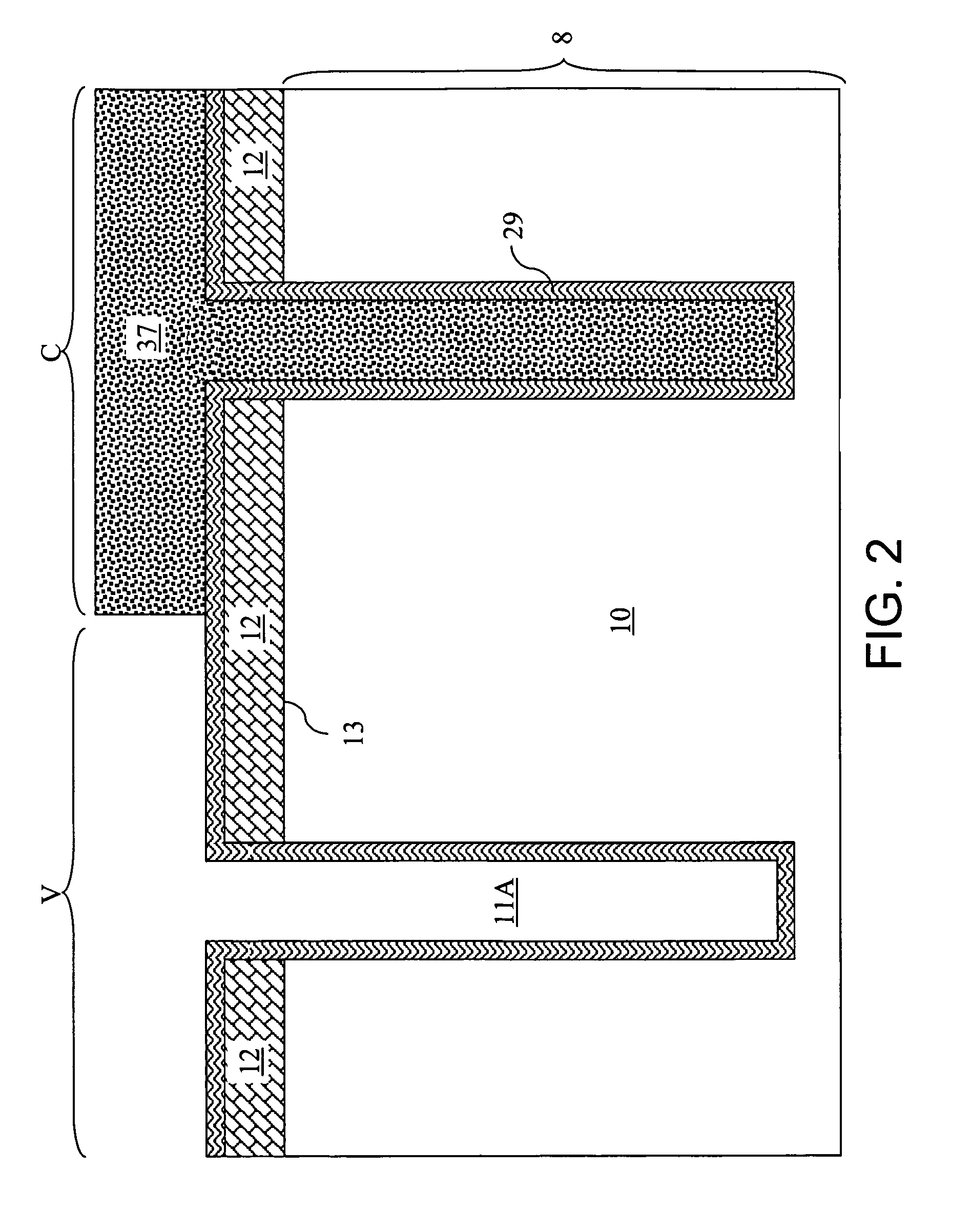
Figure 3
Abstract
Description
FIELD OF THE INVENTION
[0001] The present invention relates to a semiconductor structure, and particularly to deep trench varactors compatible with deep trench linear capacitors and methods of manufacturing the same.BACKGROUND OF THE INVENTION
[0002] A varactor is a semiconductor device having a voltage-sensitive capacitance. Frequently, the space-charge region and the accumulation at the surface of a semiconductor contacting an insulator are altered as a function of applied voltage to produce a bias-dependent capacitance.
[0003] The variability of the capacitance in a varactor may be advantageously employed in various electronic circuits to provide useful functions in amplifiers, oscillators, and frequency synthesizers. For example, varactors may be used to construct voltage-controlled oscillators (VCO), which generates a tunable stable frequency without employing a circuit with multiple oscillators. U.S. Pat. No. 7,129,801 to Wu shows an exemplary use of a varactor in a VCO circuit. A V...
Examples
first embodiment
[0079]Referring to FIG. 1, a first exemplary semiconductor structure according to the present invention comprises a semiconductor substrate 8 containing a semiconductor region 10, a first deep trench 11A, and a second deep trench 11B. Preferably, the semiconductor region 10 comprises a single crystalline semiconductor material. The semiconductor material may be selected from, but is not limited to, silicon, germanium, silicon-germanium alloy, silicon carbon alloy, silicon-germanium-carbon alloy, gallium arsenide, indium arsenide, indium phosphide, III-V compound semiconductor materials, II-VI compound semiconductor materials, organic semiconductor materials, and other compound semiconductor materials. Typically, the semiconductor material comprises silicon. Preferably, the semiconductor substrate 8 is a single crystalline substrate in which the entirety of the semiconductor region 10 is epitaxially aligned single crystalline material. The semiconductor substrate 8 may be a bulk subs...
third embodiment
[0111]Referring to FIG. 11, a third exemplary semiconductor structure according to the present invention is derived from the first exemplary semiconductor structure by formation of a second doped well 60 and a first reachthrough 62 providing electrical contact to the second doped well 60. The second doped well 60 and the first reachthrough 62 are formed by masked ion implantation. The second doped well 60 is formed directly underneath the first doped well 50. The depth of the bottom surface of the second doped well 60, which is herein referred to as a third depth d3, is greater than the second depth d2 (See FIG. 7) and less than the first depth d1. The third depth d3 may be from about 200 nm to about 2,000 nm, and typically from about 400 nm to about 1,500 nm, although lesser and greater depths are also contemplated herein. The second doped well 60 and the first doped well 50 have different dopant concentrations or different doping conductivity types. The second doped well 60 has th...
fourth embodiment
[0117]Referring to FIG. 12, a fourth exemplary semiconductor structure according to the present invention is derived from the third exemplary semiconductor structure by formation of a third doped well 70 and a second reachthrough 72 providing electrical contact to the third doped well 60. The third doped well 70 and the second reachthrough 72 are formed by masked ion implantation. The third doped well 70 is formed directly underneath the second doped well 60. The depth of the bottom surface of the third doped well 70, which is herein referred to as a fourth depth d4, is greater than the third depth d3 (See FIG. 11) and less than the first depth d1. The fourth depth d4 may be from about 300 nm to about 2,000 nm, and typically from about 600 nm to about 2,000 nm, although lesser and greater depths are also contemplated herein. The third doped well 70 has a different dopant concentration or a different doping conductivity type than the first doped well 50. The third doped well 70 has a...