
Optical storage medium comprising tracks with positive and negative marks, and stampers and production methods for manufacturing of the optical storage medium
a technology of optical storage medium and positive and negative marks, which is applied in the field of optical storage medium, can solve the problems of reducing the effective size of the light spot used for reading or writing to the optical storage medium, and not allowing to reduce the track pitch, so as to achieve the effect of reducing the effective period of the track pitch, and reducing the track pitch between two neighboring tracks
Patent Information
- Authority / Receiving Office
- US · United States
- Patent Type
- Patents(United States)
- Current Assignee / Owner
- Publication Date
- 2011-09-20
- Estimated Expiration
- Not applicable · inactive patent
Smart Images
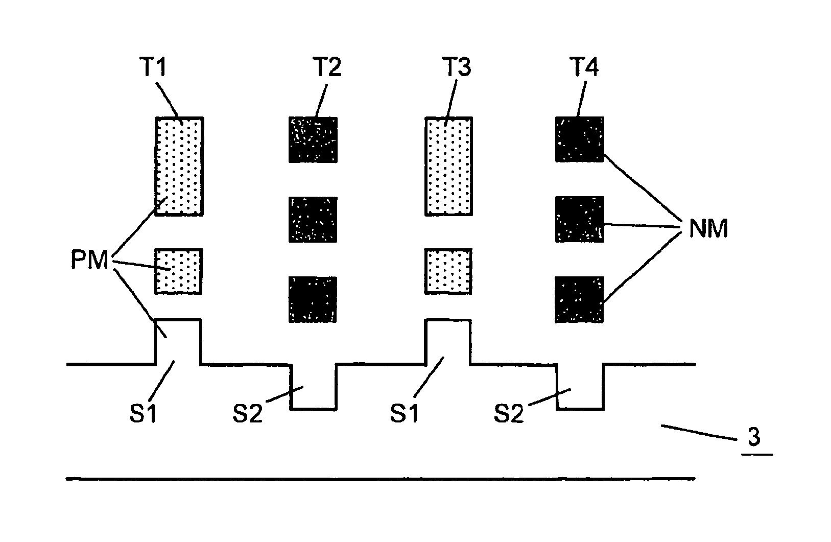
Figure 1 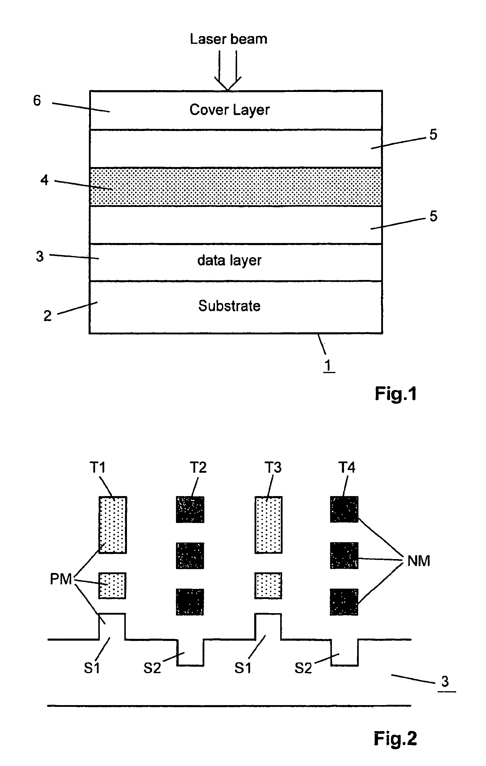
Figure 2 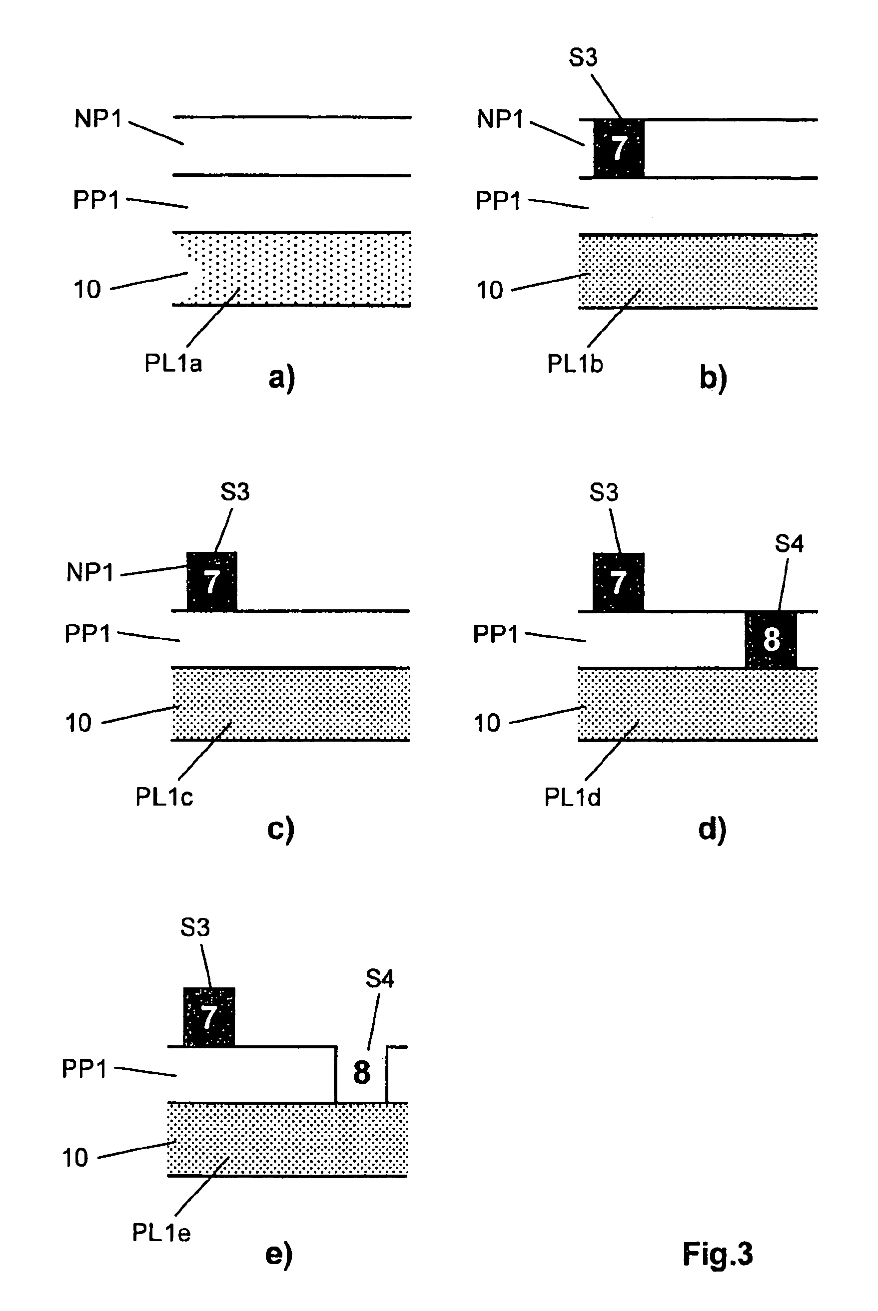
Figure 3
Abstract
Description
[0001] This application claims the benefit, under 35 U.S.C. §365 of International Application PCT / EP2007 / 060826, filed Oct. 11, 2007, which was published in accordance with PCT Article 21(2) on Apr. 24, 2008 in English and which claims the benefit of European patent application No. 06122316.0, filed Oct. 16, 2006 and European patent application No. 06123931.5, filed Nov. 13, 2006.TECHNICAL FIELD OF THE INVENTION
[0002] The present invention relates to an optical storage medium, which comprises a substrate layer, a read-only data layer with a mark / space structure arranged in tracks on the substrate layer and a cover layer, and to a respective production of the optical storage medium. The optical storage medium comprises in particular also a mask layer with a super resolution near field structure for storing of data with a high data density.BACKGROUND OF THE INVENTION
[0003] Optical storage media are media in which data are stored in an optically readable manner, for example by means of a ...
Examples
Embodiment Construction
[0021]In FIG. 1 a read-only optical storage medium 1 is shown in a cross section in a simplified manner. On a substrate 2 a read-only data layer 3 is arranged comprising a reflective metallic layer, for example an aluminum layer, data layer 3 having a data structure consisting of marks and spaces arranged on essentially parallel tracks. On the data layer 3 a first dielectric layer 5 is arranged and on the dielectric layer 5 a mask layer 4 is arranged for providing a super-resolution near-field effect (Super-RENS). The optical storage medium 1 is in particular an optical disc having a size similar to DVDs and CDs for example.
[0022]Above the mask layer 4 a second dielectric layer 5 is arranged. As a further layer, a cover layer 6 is arranged on the second dielectric layer 5 as a protective layer. For reading the data of the data layer, 3, a laser beam is applied from the top of the storage medium 1, penetrating first the cover layer 6. The first and second dielectric layers 5 comprise...