
Image sensor and method of fabricating the same
a technology of image sensor and manufacturing method, which is applied in the field of image sensor, can solve problems such as reducing sensitivity, and achieve the effect of improving reliability and productivity, and improving reliability and productivity
Patent Information
- Authority / Receiving Office
- US · United States
- Patent Type
- Patents(United States)
- Current Assignee / Owner
- Publication Date
- 2013-04-23
- Estimated Expiration
- Not applicable · inactive patent
Smart Images
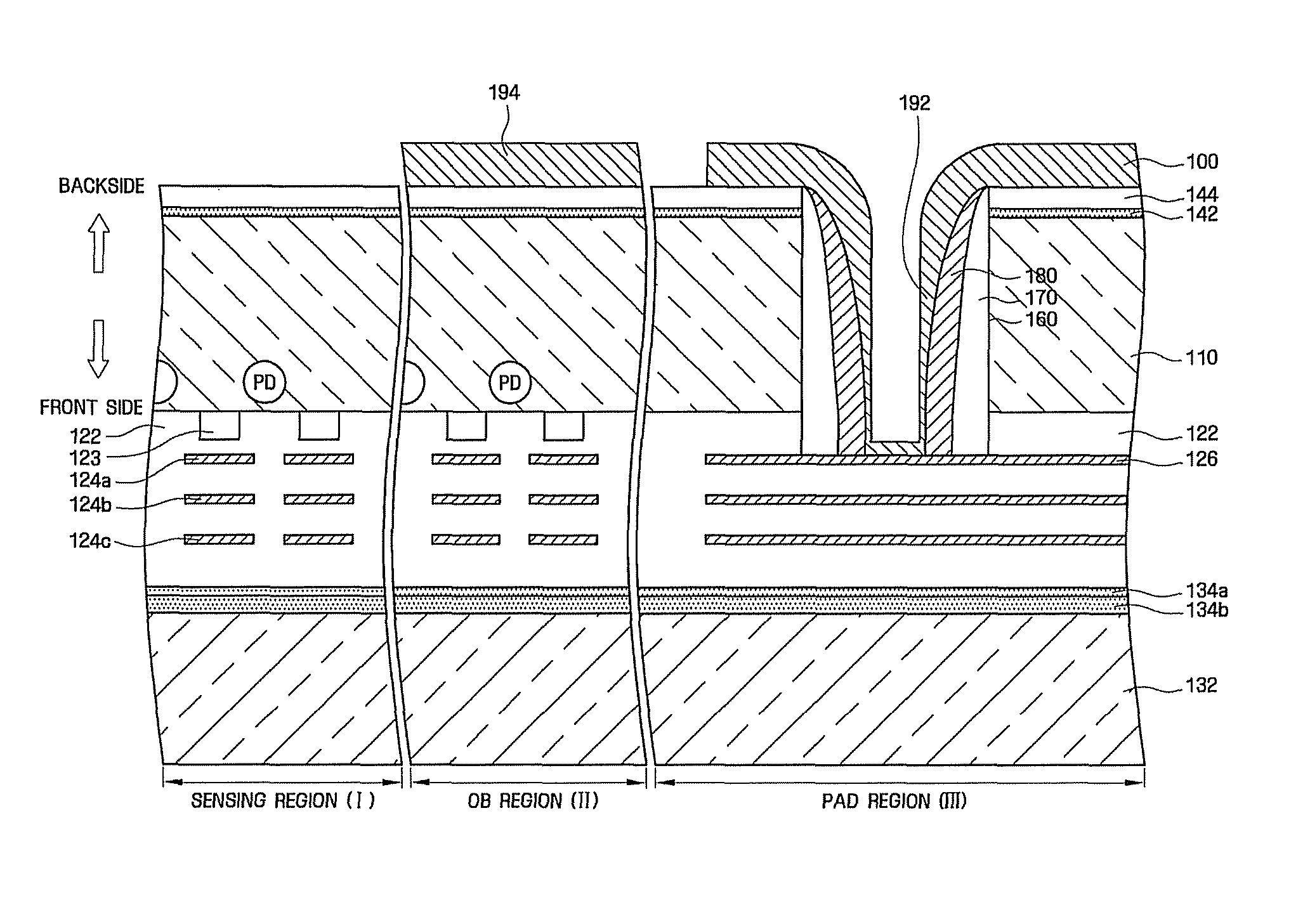
Figure 1 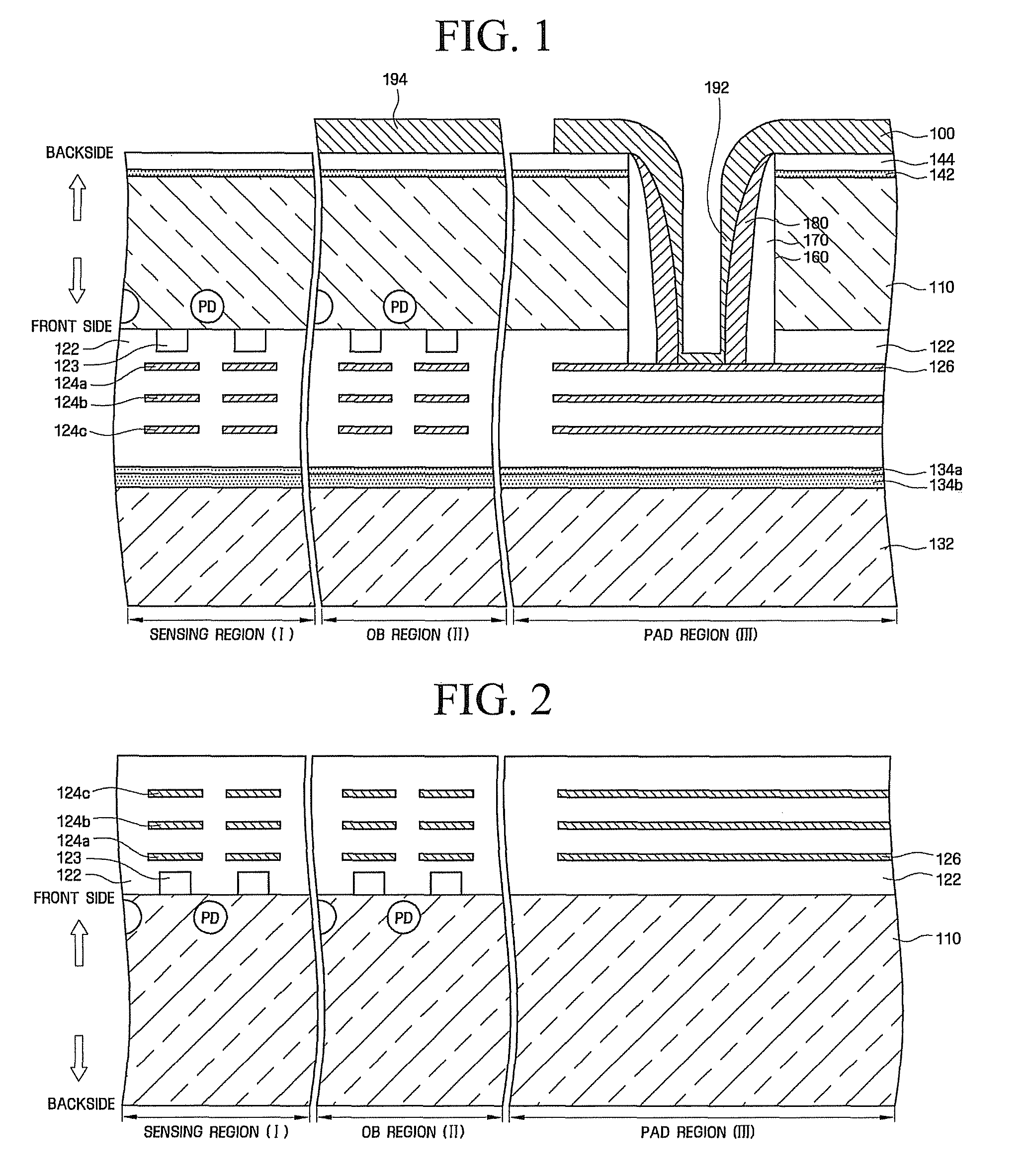
Figure 2 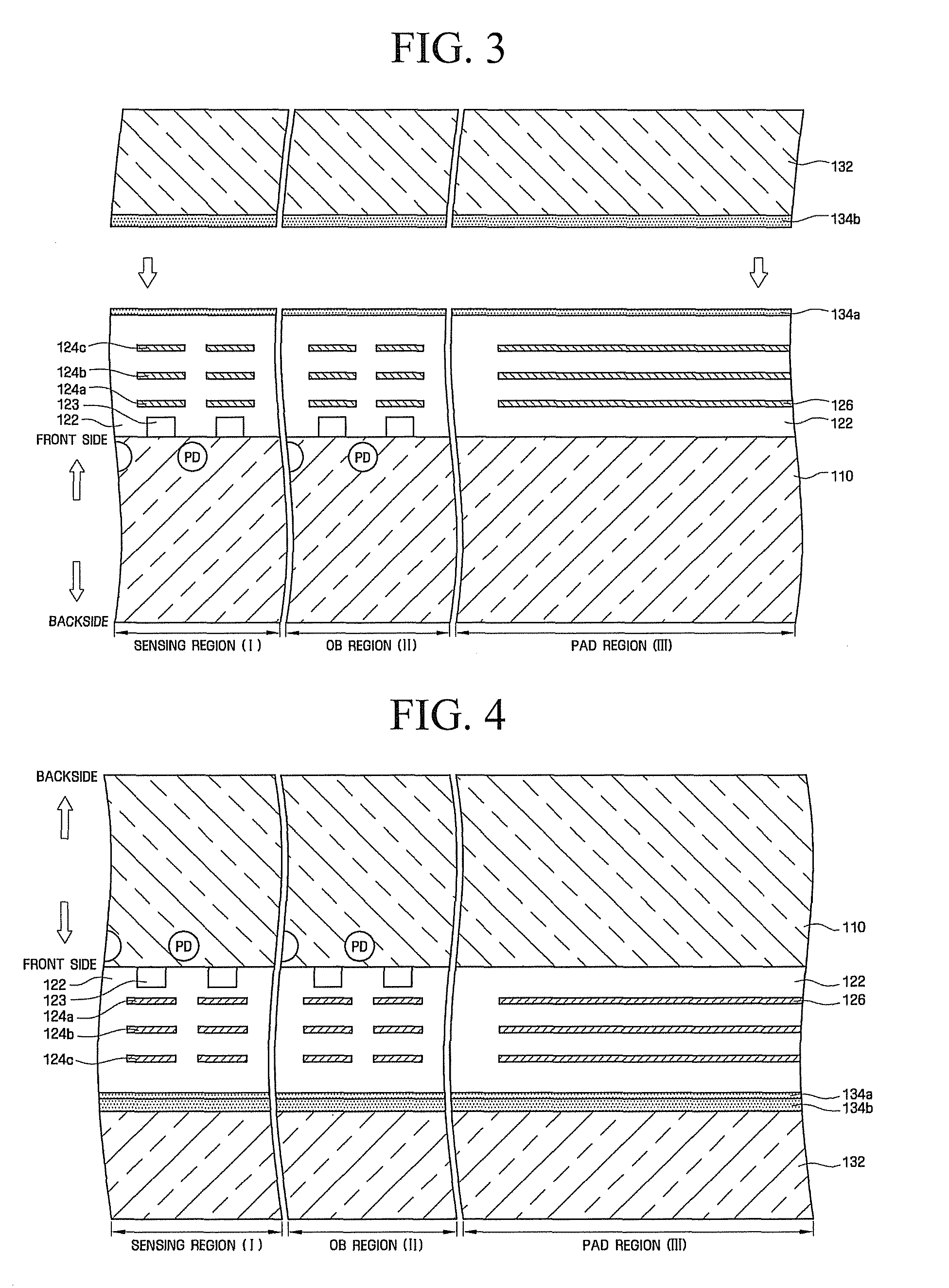
Figure 3
Abstract
Description
CROSS REFERENCE TO RELATED APPLICATION
[0001] This application claims priority under U.S.C. §119 to Korean Patent Application Nos. 10-2009-0012516 filed on Feb. 16, 2009, and 10-2009-0016948 filed on Feb. 27, 2009, in the Korean Intellectual Property Office (KIPO), the entire contents of all of which are incorporated herein by reference.BACKGROUND
[0002] 1. Field
[0003] Example embodiments of the inventive concepts relate to an image sensor and a method of fabricating the same, and more particularly, to an image sensor having improved reliability and productivity and a method of fabricating the image sensor.
[0004] 2. Description of the Related Art
[0005] Image sensors are devices that convert an optical image into an electrical signal. With recent advancements in computer and communication industries, the demands for image sensors with enhanced performance are increasing in various fields such as digital cameras, camcorders, personal communication systems, game devices, security cameras, mic...
Examples
Embodiment Construction
[0023]Advantages and features of the inventive concepts and methods of accomplishing the same may be understood more readily by reference to the following detailed description of example embodiments and the accompanying drawings. The inventive concepts may, however, be embodied in many different forms and should not be construed as being limited to the embodiments set forth herein. Rather, these embodiments are provided so that this disclosure will be thorough and complete and will fully convey the concept of the invention to those skilled in the art, and the inventive concepts will only be defined by the appended claims. In some embodiments, well-known processing processes, well-known structures and well-known technologies will not be specifically described in order to avoid ambiguous interpretation of the inventive concepts.
[0024]It will be understood that when an element or layer is referred to as being “connected to” or “coupled to” another element or layer, it can be directly c...