Accurate Measurement Methods For Switching Losses In GaN Power Devices
AUG 26, 20259 MIN READ
Generate Your Research Report Instantly with AI Agent
Patsnap Eureka helps you evaluate technical feasibility & market potential.
GaN Power Device Switching Loss Measurement Background and Objectives
Gallium Nitride (GaN) power devices have emerged as a revolutionary technology in power electronics, offering significant advantages over traditional silicon-based semiconductors. The evolution of GaN technology spans several decades, beginning with fundamental research in the 1990s and accelerating rapidly in the 2010s with commercial availability. This wide-bandgap semiconductor material enables devices that operate at higher frequencies, temperatures, and voltages while maintaining exceptional efficiency.
The accurate measurement of switching losses in GaN power devices represents a critical technical challenge that directly impacts the advancement of high-efficiency power conversion systems. Unlike silicon devices, GaN transistors exhibit ultra-fast switching speeds with transition times in the nanosecond range, making conventional measurement techniques inadequate. The extremely high dv/dt and di/dt rates during switching events create significant measurement difficulties, including parasitic inductance effects, common-mode noise, and bandwidth limitations in measurement equipment.
Current technical trends indicate a growing focus on developing specialized measurement methodologies specifically tailored to GaN's unique characteristics. The industry is moving toward integrated measurement solutions that combine high-bandwidth oscilloscopes, specialized current sensors, and advanced signal processing techniques to capture the rapid switching transitions accurately. Additionally, there is increasing interest in calorimetric measurement approaches as complementary verification methods.
The primary objective of accurate GaN switching loss measurement is to enable precise characterization of device performance under realistic operating conditions. This includes quantifying turn-on and turn-off losses, evaluating the impact of parasitic elements, and understanding loss mechanisms across various operating parameters such as temperature, voltage, and current levels. Such measurements are essential for optimizing device design, improving thermal management strategies, and maximizing overall system efficiency.
Furthermore, standardized and reliable measurement methodologies are crucial for meaningful benchmarking between different GaN technologies and manufacturers. The lack of universally accepted measurement protocols currently hampers direct performance comparisons and slows industry-wide adoption. Establishing such standards represents a key technical goal that would accelerate GaN implementation across various applications.
The ultimate technical objective extends beyond mere device characterization to enabling data-driven design optimization of GaN-based power systems. Accurate switching loss data serves as foundational input for modeling and simulation tools, allowing engineers to predict system performance and reliability with high confidence. This capability is particularly valuable for emerging applications in electric vehicles, renewable energy systems, and data center power supplies, where efficiency improvements of even fractions of a percent translate to significant energy savings.
Market Demand Analysis for High-Efficiency GaN Power Electronics
The global market for GaN power electronics is experiencing unprecedented growth, driven by the increasing demand for high-efficiency power conversion systems across multiple industries. Current market valuations place the GaN power device sector at approximately 1.4 billion USD in 2023, with projections indicating a compound annual growth rate (CAGR) of 25% through 2030. This remarkable expansion reflects the urgent need for more efficient power management solutions in an increasingly energy-conscious world.
The automotive sector represents one of the most significant market opportunities for GaN power devices. With electric vehicle (EV) production accelerating globally, manufacturers are seeking more efficient power conversion technologies to extend range and reduce charging times. GaN-based onboard chargers and DC-DC converters can achieve efficiency improvements of 3-5% compared to silicon alternatives, translating to meaningful range extensions and reduced battery requirements.
Consumer electronics constitutes another substantial market segment, with manufacturers of smartphones, laptops, and other portable devices adopting GaN-based fast chargers to deliver superior charging speeds while reducing form factors. The market penetration in this segment has grown from under 10% in 2020 to over 30% in 2023, highlighting the rapid consumer adoption of this technology.
Industrial power systems and renewable energy applications represent emerging high-growth segments. Solar inverters utilizing GaN technology demonstrate efficiency improvements of 1-2% over traditional solutions, which translates to significant energy savings at scale. The data center industry, facing mounting pressure to reduce energy consumption, has begun adopting GaN-based power supplies to improve efficiency metrics and reduce cooling requirements.
Market research indicates that accurate measurement and characterization of switching losses in GaN devices has become a critical bottleneck in the development cycle. Engineering teams report that traditional measurement techniques developed for silicon devices often fail to capture the ultra-fast switching dynamics of GaN transistors, leading to suboptimal designs and delayed time-to-market.
A survey of power electronics engineers conducted in 2023 revealed that 78% consider improved measurement methodologies for GaN switching losses as "very important" or "critical" to their development efforts. This underscores the market need for specialized test equipment, standardized measurement protocols, and advanced modeling techniques specifically tailored to GaN's unique characteristics.
The geographical distribution of market demand shows particular strength in regions with established electronics manufacturing bases and aggressive energy efficiency regulations, including East Asia, North America, and Western Europe. China, Japan, and South Korea collectively represent over 45% of the current market demand, driven by their dominant positions in consumer electronics manufacturing and electric vehicle production.
Current Challenges in GaN Switching Loss Measurement Techniques
Despite significant advancements in GaN power device technology, accurate measurement of switching losses remains a formidable challenge for researchers and engineers. The ultra-fast switching speeds of GaN devices, often in the sub-nanosecond range, create fundamental measurement difficulties that conventional techniques struggle to address. Current measurement systems face bandwidth limitations, with most oscilloscopes and voltage probes operating below the required bandwidth for capturing GaN's rapid transitions accurately.
Signal integrity issues present another major obstacle. The high dv/dt and di/dt rates in GaN switching events generate substantial electromagnetic interference, leading to measurement distortions. Common mode currents flowing through probe ground loops and parasitic capacitances introduce significant measurement errors that can exceed the actual switching losses being measured.
Temperature dependency further complicates accurate assessment. GaN device characteristics vary considerably with temperature, yet most measurement setups lack precise temperature control capabilities. This creates inconsistencies when comparing measurements across different operating conditions or between research groups.
Parasitic elements in measurement circuits represent perhaps the most persistent challenge. Even minimal inductance in current shunts or capacitance in voltage probes can dramatically alter the switching behavior being measured. The "observer effect" becomes pronounced, where the act of measurement itself modifies the circuit behavior being studied.
Calibration standards specific to high-speed GaN measurements remain underdeveloped. While calibration methods exist for silicon-based power devices, these prove inadequate for the extreme switching speeds of GaN technology. The lack of standardized calibration procedures leads to significant variations in reported switching loss data across the industry.
Data processing methodologies also present challenges. The extraction of true switching losses from measured waveforms requires sophisticated de-embedding techniques to account for measurement system artifacts. Different research groups employ varying data processing approaches, making direct comparison of published results problematic.
The dynamic on-resistance (Ron) measurement in GaN devices presents unique difficulties. The current collapse phenomenon in GaN HEMTs causes Ron to vary dynamically during switching events, yet conventional measurement techniques typically capture only static Ron values, leading to underestimation of actual switching losses.
These challenges collectively create a significant barrier to the widespread industrial adoption of GaN technology. Without reliable, standardized measurement techniques, design engineers cannot accurately predict system performance or confidently compare GaN solutions against established silicon alternatives, ultimately slowing market penetration despite GaN's inherent performance advantages.
State-of-the-Art Switching Loss Measurement Solutions
01 Device structure optimization for reducing switching losses
GaN power devices can be designed with optimized structures to minimize switching losses. These optimizations include improved gate designs, reduced parasitic capacitances, and enhanced channel mobility. By carefully engineering the device structure, the charge required for switching can be reduced, leading to faster switching speeds and lower switching losses. These structural improvements enable GaN devices to operate efficiently at high frequencies while maintaining thermal stability.- Gate driver optimization for GaN devices: Optimizing gate driver circuits for GaN power devices can significantly reduce switching losses. This includes implementing precise gate voltage control, optimizing gate resistance values, and using advanced gate driver ICs specifically designed for GaN devices. These techniques help to minimize the turn-on and turn-off times, reducing the overlap between voltage and current during switching transitions, which is a major source of switching losses in GaN power devices.
- Device structure improvements to reduce parasitic capacitance: Modifications to the physical structure of GaN power devices can reduce parasitic capacitances, which directly impact switching losses. These improvements include optimized field plate designs, reduced gate-to-drain overlap, and enhanced channel structures. By minimizing parasitic capacitances, especially the gate-to-drain capacitance (Cgd), the charging and discharging energy during switching transitions is reduced, leading to lower switching losses and faster switching speeds.
- Advanced packaging and thermal management techniques: Innovative packaging and thermal management solutions can help reduce switching losses in GaN power devices. These include low-inductance package designs, integrated cooling solutions, and optimized layout techniques that minimize parasitic inductances in the power loop. Effective thermal management also allows GaN devices to operate at lower temperatures, which can improve their switching performance and reduce losses associated with increased resistance at higher temperatures.
- Circuit topology and layout optimization: The design of power conversion circuit topologies and PCB layouts significantly impacts switching losses in GaN power devices. Optimized circuit topologies like bridgeless PFC, multilevel converters, and resonant soft-switching circuits can reduce switching stress. Additionally, minimizing power loop inductance through careful PCB layout, using optimal decoupling capacitor placement, and implementing symmetrical designs helps reduce ringing and overshoot during switching transitions, thereby decreasing switching losses.
- Switching loss measurement and modeling techniques: Advanced measurement and modeling techniques are essential for accurately characterizing and predicting switching losses in GaN power devices. These include double-pulse testing methods, calorimetric measurement approaches, and sophisticated simulation models that account for parasitic elements and dynamic behavior. Accurate measurement and modeling enable designers to optimize operating conditions, identify loss mechanisms, and develop strategies to minimize switching losses in GaN-based power conversion systems.
02 Gate driver design and control strategies
Advanced gate driver designs and control strategies play a crucial role in minimizing switching losses in GaN power devices. Optimized gate drivers can provide precise control of turn-on and turn-off transitions, reducing overlap between voltage and current during switching events. Techniques such as adaptive gate driving, multi-level gate control, and resonant gate driving can significantly reduce switching losses by managing the gate charge more efficiently and controlling the switching speed according to operating conditions.Expand Specific Solutions03 Thermal management techniques
Effective thermal management is essential for controlling switching losses in GaN power devices. As switching losses generate heat, improved thermal dissipation methods such as advanced packaging technologies, integrated heat spreaders, and optimized thermal interfaces can help maintain lower operating temperatures. Lower junction temperatures reduce on-resistance and switching losses, improving overall efficiency and reliability of GaN power devices, especially under high-frequency switching conditions.Expand Specific Solutions04 Circuit topology and layout optimization
The circuit topology and layout significantly impact switching losses in GaN power devices. Minimizing parasitic inductances and capacitances through optimized PCB layouts, shorter interconnections, and improved power loop designs can substantially reduce switching losses. Advanced topologies such as soft-switching circuits, resonant converters, and multilevel configurations can be implemented to reduce the stress on GaN devices during switching transitions, thereby decreasing overall switching losses and improving system efficiency.Expand Specific Solutions05 Material innovations and fabrication techniques
Advancements in material science and fabrication techniques contribute to reducing switching losses in GaN power devices. Innovations such as improved epitaxial growth methods, novel buffer layer designs, and enhanced passivation techniques can reduce defect densities and improve interface quality. These improvements lead to reduced trap-related losses, lower dynamic on-resistance, and better switching performance. Additionally, the integration of complementary materials with GaN can create heterojunctions with superior electron transport properties, further reducing switching losses.Expand Specific Solutions
Leading Players in GaN Power Device Testing Equipment
The GaN power device switching loss measurement market is in a growth phase, characterized by increasing adoption of GaN technology in power electronics due to its superior performance over silicon. The global market is expanding rapidly, driven by electric vehicle adoption, renewable energy integration, and data center power demands. Technical maturity varies across players, with companies like Wolfspeed, Innoscience, and ROHM leading in commercial GaN device development. Academic institutions including Shanghai Jiao Tong University, Xidian University, and University of Electronic Science & Technology of China are advancing measurement methodologies, while industrial players such as Huawei, TDK, and Infineon Technologies Austria are integrating these techniques into product development. The ecosystem shows a collaborative approach between academia and industry to standardize accurate measurement techniques for GaN switching losses.
Infineon Technologies Austria AG
Technical Solution: Infineon has pioneered a multi-tiered approach to GaN switching loss measurement that addresses the unique challenges posed by these high-speed devices. Their methodology combines traditional double-pulse testing with advanced compensation techniques that account for the voltage-dependent capacitances and nonlinear behavior of GaN devices. Infineon's system utilizes ultra-high bandwidth oscilloscopes (>1 GHz) coupled with specialized deskewing procedures to ensure precise time alignment between voltage and current measurements[3]. A key innovation in their approach is the development of a "dynamic RON" characterization technique that captures the charge-trapping effects specific to GaN devices, which can significantly impact switching loss measurements over time and temperature. Their test fixtures incorporate coaxial shunt resistors with extremely low inductance (<1nH) and specialized gate drivers optimized to minimize common-mode noise interference during measurement. Infineon also employs sophisticated numerical integration algorithms that account for the energy stored in parasitic components, providing a more accurate representation of the actual device losses rather than circuit losses[5].
Strengths: Comprehensive approach addressing GaN-specific phenomena like dynamic RON and charge trapping effects; industry-standard measurement systems with excellent repeatability and temperature compensation. Weakness: Their methods often require complex calibration procedures that must be frequently repeated to maintain measurement accuracy, increasing testing time and complexity.
ROHM Co., Ltd.
Technical Solution: ROHM has developed a proprietary switching loss measurement system specifically designed for their GaN power device portfolio. Their approach centers on a custom-designed low-inductance test board with integrated current sensing capabilities that minimize measurement loop inductance to less than 2nH. ROHM's methodology incorporates a time-domain correction algorithm that compensates for the phase delays between voltage and current measurements, which is particularly critical for GaN devices where switching transitions occur in nanoseconds[2]. Their system employs specialized wide-bandwidth current sensors based on Rogowski coils with flat frequency response up to 300MHz to accurately capture the high di/dt events characteristic of GaN switching. ROHM has also implemented an innovative "energy balance verification" technique that cross-validates switching loss measurements against total power dissipation measured through thermal methods, providing an important consistency check. Additionally, they've developed specific test protocols for different GaN device structures (e-mode vs cascode) that account for the unique switching behaviors of each architecture, ensuring accurate characterization across their entire product line[4].
Strengths: Purpose-built measurement systems optimized for different GaN device architectures; excellent noise immunity through careful shielding and grounding techniques. Weakness: Their methodology may be overly optimized for ROHM's specific device structures and packaging, potentially limiting applicability to other manufacturers' GaN devices.
Critical Patents and Research in GaN Measurement Technology
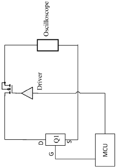
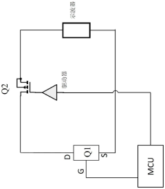
Apparatus and method for measuring dynamic on-resistance of nitride-based switching device
PatentWO2023164900A1
Innovation
- Development of a specialized testing apparatus that addresses oscilloscope measurement overshoot issues when measuring GaN device dynamic on-resistance, enabling more accurate power loss modeling.
- Implementation of a controller-based system that precisely times the measurement of drain-source voltage during the conduction interval, avoiding the transition periods where voltage fluctuations are most severe.
- Design of a measurement methodology that can accurately capture the millivolt-level drain-source voltage during on-state while handling the high voltage levels during off-state without compromising measurement accuracy.
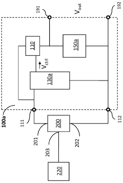
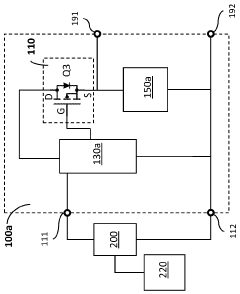
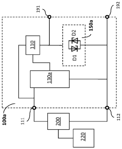
Apparatus and method for measuring dynamic on-resistance of nitride-based switching devices
PatentActiveCN114729958B
Innovation
- A device including an input interface, an output interface, a clamp module and a drive module is designed. Through the electrical coupling of the clamp module and the drive module, the state changes are sensed and a control signal is generated to turn on and off the clamp module to ensure that the output voltage is within Indicates drain-source voltage when clamped to avoid overshoot.
Thermal Management Considerations in GaN Measurement Systems
Thermal management represents a critical aspect of accurate measurement systems for GaN power devices, as temperature variations can significantly impact switching loss measurements. GaN devices, while offering superior performance compared to silicon counterparts, generate substantial heat during high-frequency switching operations that must be properly managed to ensure measurement accuracy.
The thermal conductivity of GaN (130 W/m·K) exceeds that of silicon, yet thermal management remains challenging due to the high power density and fast switching capabilities of these devices. During switching loss measurements, even minor temperature fluctuations can alter device characteristics, introducing measurement errors that compromise data reliability. Research indicates that a 10°C temperature increase can result in up to 8% variation in switching losses for GaN devices.
Effective thermal management systems typically incorporate multiple cooling mechanisms. Active cooling solutions, including forced-air and liquid cooling systems, have demonstrated superior performance in laboratory settings. Recent advancements in microchannel liquid cooling have shown particular promise, achieving thermal resistances below 0.1°C/W in high-power measurement setups.
Temperature monitoring represents another crucial component of thermal management in measurement systems. High-precision infrared thermal imaging and integrated temperature sensors enable real-time monitoring of device temperature during switching events. These monitoring systems should feature response times under 1ms to capture transient thermal behaviors that may affect measurement accuracy.
The physical layout of measurement systems also significantly impacts thermal performance. Optimal designs minimize thermal resistance between the device under test and cooling mechanisms. Advanced thermal interface materials (TIMs) with thermal conductivities exceeding 5 W/m·K have been implemented in recent measurement platforms to enhance heat transfer efficiency.
Calibration procedures must account for thermal effects to ensure measurement accuracy. Temperature compensation algorithms that adjust measurement parameters based on real-time temperature data have demonstrated improved accuracy in recent studies. These algorithms typically incorporate device-specific thermal models derived from extensive characterization data.
Future developments in thermal management for GaN measurement systems will likely focus on integrated cooling solutions that combine multiple cooling mechanisms with advanced thermal monitoring capabilities. Machine learning approaches for predictive thermal management also show promise, potentially enabling dynamic adjustment of measurement parameters based on anticipated thermal behavior.
Standardization Efforts for GaN Power Device Testing
The standardization of testing methodologies for GaN power devices has become increasingly critical as these devices gain wider adoption across various industries. Currently, several international organizations are actively working to establish unified testing protocols specifically for GaN technology. The Joint Electron Device Engineering Council (JEDEC) has formed dedicated working groups focused on wide bandgap semiconductors, with specific attention to GaN power device characterization and reliability assessment methods.
IEEE has also contributed significantly through its Power Electronics Society, developing standards such as IEEE P2823, which addresses test procedures for GaN-based power conversion devices. This standard aims to provide consistent methodologies for measuring switching losses, a particularly challenging aspect of GaN device characterization due to their ultra-fast switching speeds.
The International Electrotechnical Commission (IEC) has been working on extending existing power semiconductor testing standards to accommodate the unique characteristics of GaN devices. Their efforts include adapting traditional MOSFET and IGBT testing protocols to address the specific behaviors of GaN technology, particularly regarding dynamic on-resistance and switching performance evaluation.
Regional standardization bodies have also joined these efforts. In Europe, CENELEC has initiated projects to harmonize GaN testing approaches across EU member states, while in Asia, organizations like JEITA in Japan and CESI in China are developing region-specific guidelines that align with global standards while addressing local industry needs.
Industry consortia play a crucial role in these standardization efforts. The PowerAmerica Institute, Compound Semiconductor Applications Catapult, and the European Center for Power Electronics have established collaborative platforms where device manufacturers, test equipment providers, and end-users collectively develop and validate measurement methodologies.
A key focus of these standardization initiatives is addressing the unique challenges in measuring switching losses in GaN devices. These include establishing protocols for ultra-high-speed measurement systems capable of accurately capturing nanosecond-scale switching events, defining standard test circuits that minimize parasitic elements, and creating reference waveforms for validation of measurement accuracy.
The development of standardized double-pulse test configurations specifically optimized for GaN devices represents a significant advancement, as these tests must account for much faster dv/dt and di/dt rates than traditional silicon-based testing. Additionally, efforts are underway to standardize calorimetric measurement approaches as complementary verification methods for electrical switching loss measurements.
Unlock deeper insights with Patsnap Eureka Quick Research — get a full tech report to explore trends and direct your research. Try now!
Generate Your Research Report Instantly with AI Agent
Supercharge your innovation with Patsnap Eureka AI Agent Platform!