Reliability Qualification Of GaN Power Devices Including HTOL, HV/H3TRB, And Solder Fatigue
AUG 26, 20259 MIN READ
Generate Your Research Report Instantly with AI Agent
Patsnap Eureka helps you evaluate technical feasibility & market potential.
GaN Power Device Reliability Background and Objectives
Gallium Nitride (GaN) power devices have emerged as a revolutionary technology in the power electronics industry over the past two decades. The wide bandgap semiconductor material offers superior properties compared to traditional silicon-based devices, including higher breakdown voltage, faster switching speeds, lower on-resistance, and better thermal conductivity. These advantages enable more efficient power conversion systems with reduced size and weight, making GaN particularly attractive for applications in electric vehicles, renewable energy systems, data centers, and consumer electronics.
The evolution of GaN power technology has progressed through several significant phases. Initially developed for RF and optoelectronic applications in the 1990s, GaN's potential for power electronics was recognized in the early 2000s. The subsequent decade saw intensive research efforts focused on overcoming material quality issues and developing viable device structures. By the 2010s, commercial GaN power devices began entering the market, primarily in the form of high-electron-mobility transistors (HEMTs).
Despite the promising performance characteristics, reliability concerns have been a major barrier to widespread adoption of GaN power devices. Unlike silicon technology with decades of reliability data, GaN devices present unique degradation mechanisms that require thorough understanding and qualification. The industry has been working to establish standardized reliability testing protocols specifically tailored to GaN's unique material properties and failure modes.
The primary objective of reliability qualification for GaN power devices is to ensure their long-term performance stability under various operational and environmental stresses. High-Temperature Operating Life (HTOL) testing evaluates device degradation under elevated temperatures and electrical stress, simulating accelerated aging conditions. High-Voltage/High-Humidity Temperature Reverse Bias (HV/H3TRB) testing assesses susceptibility to moisture-induced failures, particularly critical for GaN's unique surface-sensitive characteristics. Solder fatigue testing examines the mechanical integrity of device packaging under thermal cycling conditions.
Current reliability qualification efforts aim to establish industry-wide standards that accurately predict GaN device lifetime in real-world applications. This involves developing acceleration models that correlate accelerated test results with actual field performance. Additionally, there is growing interest in understanding the fundamental physics of failure mechanisms specific to GaN, including dynamic Ron degradation, threshold voltage instability, and buffer trapping effects.
The ultimate goal is to achieve reliability levels that match or exceed those of silicon devices, thereby enabling GaN technology to fulfill its potential for revolutionizing power electronics across multiple industries. This requires collaborative efforts between device manufacturers, testing laboratories, and end-users to build a comprehensive reliability knowledge base for this promising technology.
Market Demand Analysis for Reliable GaN Power Solutions
The global power electronics market is experiencing a significant shift towards Gallium Nitride (GaN) technology, with demand for reliable GaN power solutions growing exponentially. Market research indicates that the GaN power device market is projected to reach $1.75 billion by 2026, with a compound annual growth rate of approximately 35% from 2021. This remarkable growth is primarily driven by the superior performance characteristics of GaN compared to traditional silicon-based solutions, including higher efficiency, faster switching speeds, and smaller form factors.
The automotive sector represents one of the largest market segments for reliable GaN power devices, particularly with the rapid expansion of electric vehicles (EVs). EV manufacturers are actively seeking power solutions that can enhance range, reduce charging times, and minimize thermal management requirements. GaN-based onboard chargers and DC-DC converters that demonstrate proven reliability under high-temperature operating life (HTOL) conditions are experiencing particularly strong demand growth.
Consumer electronics manufacturers constitute another significant market segment, with increasing adoption of GaN technology in fast chargers, adapters, and power supplies. The miniaturization trend in consumer devices is creating substantial demand for GaN solutions that can deliver higher power density while maintaining reliability under various environmental conditions, including high humidity high temperature reverse bias (H3TRB) scenarios.
The renewable energy sector is emerging as a critical growth area for reliable GaN power devices. Solar inverters and wind power converters benefit significantly from GaN's efficiency advantages, but these applications demand exceptional reliability due to their outdoor deployment and expected operational lifespans of 20+ years. Qualification standards that address solder fatigue and long-term reliability are particularly valued by customers in this segment.
Data center and telecommunications infrastructure represents another high-growth market for GaN power solutions. The increasing power demands of server farms and 5G infrastructure, coupled with energy efficiency mandates, are driving adoption of GaN technology in power supplies and converters. These applications require devices that can demonstrate reliability under continuous high-power operation and varying environmental conditions.
Industrial automation and manufacturing systems are gradually transitioning to GaN-based power solutions to achieve higher energy efficiency and system performance. This market segment places particular emphasis on reliability qualifications, as downtime due to component failure can result in significant production losses and maintenance costs.
Market analysis reveals that customers across all segments are increasingly demanding comprehensive reliability data before adopting GaN technology. Qualification methodologies that address HTOL, HV/H3TRB, and solder fatigue are becoming key differentiators for GaN device manufacturers, with customers willing to pay premium prices for solutions with proven reliability credentials and transparent qualification data.
Current Reliability Challenges in GaN Power Semiconductors
Despite significant advancements in GaN power semiconductor technology, several critical reliability challenges persist that impede widespread commercial adoption. The dynamic nature of GaN devices, particularly under high-voltage and high-temperature conditions, presents unique degradation mechanisms not observed in traditional silicon-based semiconductors. These reliability concerns manifest differently across various device architectures including lateral HEMTs, vertical GaN structures, and hybrid configurations.
Current threshold voltage instability remains a primary concern, with both positive and negative shifts observed during high-temperature gate bias stress testing. This instability directly impacts device performance consistency and long-term reliability in power conversion applications. The root causes involve charge trapping phenomena at the gate dielectric/AlGaN interface and within the buffer layers, which continue to challenge device engineers.
Dynamic ON-resistance degradation (current collapse) presents another significant reliability hurdle. Under high-voltage switching conditions, GaN devices experience temporary increases in ON-resistance due to charge trapping effects, reducing efficiency and thermal performance. While various field plate designs and buffer optimization techniques have improved this characteristic, complete elimination remains elusive, particularly in applications requiring blocking voltages above 650V.
Time-dependent dielectric breakdown (TDDB) mechanisms in GaN power devices differ substantially from silicon counterparts, with unique failure modes observed during HTOL (High Temperature Operating Life) testing. The heterogeneous material interfaces in GaN device structures create complex electric field distributions that can accelerate dielectric degradation, especially at elevated temperatures.
Moisture sensitivity presents a particularly challenging reliability issue, as evidenced in H3TRB (High Humidity, High Temperature Reverse Bias) testing. The polar nature of III-nitride materials makes them susceptible to electrochemical reactions in the presence of moisture, potentially leading to accelerated degradation of surface passivation layers and metal contacts.
Package-related reliability concerns, particularly solder fatigue and die-attach degradation, are exacerbated by GaN's unique thermal cycling behavior. The thermal expansion coefficient mismatch between GaN, silicon substrates, and packaging materials creates mechanical stresses during power cycling that can lead to premature package failure, even when the semiconductor device itself remains functional.
Radiation hardness and cosmic ray susceptibility represent emerging reliability concerns as GaN devices penetrate aerospace, automotive, and industrial applications. Single-event burnout thresholds in GaN differ significantly from silicon devices, requiring new qualification methodologies and hardening techniques to ensure reliability in radiation-exposed environments.
Current HTOL and H3TRB Testing Approaches
01 Structural design improvements for GaN power devices
Various structural design improvements can enhance the reliability of GaN power devices. These include optimized gate structures, buffer layer designs, and field plate configurations that help distribute electric fields more evenly. Advanced packaging techniques and thermal management structures are also implemented to improve heat dissipation and reduce thermal stress. These structural enhancements collectively contribute to increased device lifetime and operational stability under high-power conditions.- Structural design improvements for GaN power devices: Various structural design improvements can enhance the reliability of GaN power devices. These include optimized gate structures, buffer layer designs, and field plate configurations that help distribute electric fields more evenly. Advanced packaging techniques and thermal management structures are also implemented to improve heat dissipation and reduce thermal stress. These structural enhancements collectively contribute to increased device lifetime and operational stability under high-power conditions.
- Passivation and surface treatment techniques: Surface passivation and treatment methods significantly impact GaN power device reliability. Specialized dielectric layers and surface treatments are applied to reduce surface states and trap densities at interfaces. These techniques help minimize current collapse, threshold voltage instability, and dynamic on-resistance issues. Advanced passivation materials and processes can effectively suppress electron trapping mechanisms and protect the device surface from environmental degradation, resulting in more stable long-term performance.
- Reliability testing and qualification methodologies: Comprehensive reliability testing and qualification methodologies are essential for evaluating GaN power device performance. These include accelerated life tests, high-temperature operating life tests, temperature cycling, and bias stress tests. Advanced characterization techniques help identify failure mechanisms and reliability concerns. Statistical analysis of test data enables lifetime prediction models and helps establish reliability standards specific to GaN technology, ensuring devices meet industry requirements for various applications.
- Thermal management solutions: Effective thermal management is crucial for GaN power device reliability. Innovative heat dissipation structures, including advanced substrates, thermal vias, and integrated heat spreaders, help maintain lower junction temperatures during operation. Novel packaging materials with high thermal conductivity and reduced thermal resistance improve heat flow away from active device regions. These thermal management solutions prevent performance degradation and extend device lifetime by mitigating temperature-related failure mechanisms.
- Material quality and epitaxial growth optimization: The quality of GaN materials and epitaxial growth processes directly impacts device reliability. Advanced growth techniques minimize crystal defects, dislocations, and impurities that can act as trapping centers or leakage paths. Buffer layer optimization reduces stress and improves lattice matching between GaN and substrates. Precise control of doping profiles and interface quality during epitaxial growth enhances carrier transport properties and breakdown characteristics, resulting in more reliable power devices with consistent performance.
02 Reliability testing and failure analysis methods
Specialized testing methodologies have been developed to evaluate and predict the reliability of GaN power devices. These include accelerated life testing, high-temperature operating life tests, and stress tests under various electrical and thermal conditions. Advanced failure analysis techniques help identify degradation mechanisms and failure modes specific to GaN technology. These testing protocols enable manufacturers to improve device designs and manufacturing processes to enhance long-term reliability.Expand Specific Solutions03 Passivation and surface treatment techniques
Surface passivation and treatment methods significantly impact GaN power device reliability. Various dielectric materials and deposition techniques are used to passivate the device surface, reducing current collapse and dynamic on-resistance. Surface treatments help mitigate trapping effects at interfaces and reduce leakage currents. These techniques effectively address reliability issues related to surface states and charge trapping phenomena that commonly affect GaN device performance over time.Expand Specific Solutions04 Thermal management solutions
Effective thermal management is crucial for GaN power device reliability. Advanced cooling solutions, including novel substrate materials with higher thermal conductivity, are implemented to dissipate heat efficiently. Thermal interface materials and optimized package designs help reduce thermal resistance. Integrated temperature sensors and thermal protection circuits prevent device failure under extreme operating conditions. These thermal management approaches significantly extend device lifetime by preventing degradation mechanisms accelerated by high temperatures.Expand Specific Solutions05 Epitaxial growth and material quality improvements
The quality of epitaxial layers fundamentally determines GaN power device reliability. Advanced growth techniques minimize crystal defects, dislocations, and impurities that can lead to premature device failure. Buffer layer optimization reduces stress and improves carrier confinement. Novel substrate materials and growth conditions help achieve higher material quality. These improvements in epitaxial growth technology directly enhance device reliability by reducing defect-related degradation mechanisms and improving overall device performance stability over time.Expand Specific Solutions
Leading Players in GaN Power Device Manufacturing
The GaN power device reliability qualification market is currently in a growth phase, with increasing adoption across automotive, telecommunications, and renewable energy sectors. The market size is expanding rapidly, driven by the superior performance of GaN over traditional silicon in high-power applications. Technologically, the field is advancing from early maturity to mainstream adoption, with companies at different development stages. Industry leaders like Infineon, Texas Instruments, and Wolfspeed have established comprehensive qualification frameworks, while newer entrants such as InnoScience and Huawei Digital Power are rapidly advancing their reliability testing capabilities. Academic-industry collaborations involving institutions like Xidian University and National Tsing-Hua University are accelerating standardization efforts for HTOL, HV/H3TRB, and solder fatigue testing methodologies, essential for widespread commercial adoption.
Huawei Technologies Co., Ltd.
Technical Solution: Huawei has developed an advanced reliability qualification framework for GaN power devices used in their telecommunications and power delivery systems. Their HTOL testing methodology incorporates both static and dynamic stress conditions at elevated temperatures (up to 175°C) with comprehensive electrical parameter monitoring to detect subtle degradation before catastrophic failure. For HV/H3TRB qualification, Huawei employs specialized test chambers with precise control of temperature and humidity gradients, critical for accurate assessment of moisture-related failure mechanisms in GaN devices. Their approach to solder fatigue qualification includes advanced thermal cycling protocols combined with real-time electrical and thermal impedance monitoring to detect early signs of package degradation[5]. Huawei has pioneered the use of machine learning algorithms to analyze reliability test data, enabling more accurate prediction of device lifetimes and identification of potential failure patterns. Their qualification framework incorporates mission profile-based testing that simulates the specific stress conditions encountered in telecommunications infrastructure, data centers, and renewable energy systems where their GaN devices are deployed.
Strengths: Extensive vertical integration allowing for system-level reliability optimization and real-world validation in their own infrastructure products. Their qualification methodology benefits from large-scale deployment data across diverse operating environments. Weaknesses: Their qualification approach may be heavily optimized for telecommunications applications, potentially overlooking some requirements for other industrial or automotive use cases.
Infineon Technologies Austria AG
Technical Solution: Infineon has established a sophisticated reliability qualification framework for GaN power devices that addresses the unique failure mechanisms of this technology. Their HTOL testing methodology incorporates not only standard temperature acceleration (up to 175°C) but also dynamic switching conditions that better represent real-world applications. For HV/H3TRB qualification, Infineon employs a multi-stage approach with intermediate characterizations to identify early indicators of degradation before catastrophic failure occurs. Their proprietary "CoolGaN" technology undergoes specialized solder fatigue testing using power cycling with ΔTj monitoring and advanced structure function analysis to detect subtle changes in thermal resistance[2]. Infineon has developed physics-of-failure models that correlate accelerated test results with field reliability, allowing for more accurate lifetime predictions. Their qualification process includes additional tests beyond standard requirements, such as surge current capability and short-circuit withstand time evaluations that are critical for industrial applications.
Strengths: Extensive experience in power semiconductor qualification with specialized equipment and methodologies tailored for GaN technology. Their reliability data is backed by large-scale field deployment experience. Weaknesses: Their qualification approach tends to be conservative, potentially over-designing for reliability at the expense of performance optimization in certain applications.
Critical Analysis of GaN Failure Mechanisms
Gallium nitride component, method for manufacturing gallium nitride component, and electronic device
PatentPendingUS20240204094A1
Innovation
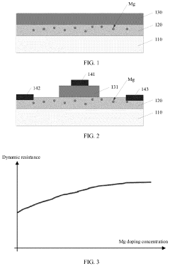
- A gallium nitride component is designed with a barrier layer composed of aluminum, gallium, and nitrogen, where the layer's size and aluminum concentration gradient in the gate region naturally exhaust electrons without Mg doping, reducing the risk of dynamic resistance degradation and maintaining channel integrity.
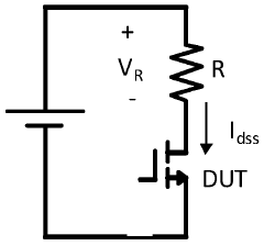
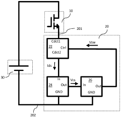
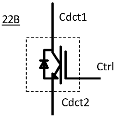
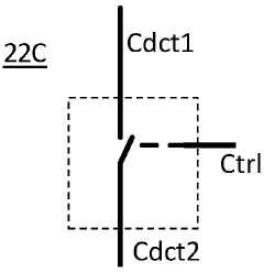
Protection circuit for high temperature reverse bias test
PatentWO2024000186A1
Innovation
- Implementation of a current-limiting resistor in series with each GaN device under test to passively reduce leakage current during HTRB testing, preventing catastrophic failure and simplifying failure analysis.
- Parallel connection configuration for multiple GaN devices under test with individual protection mechanisms to isolate failed devices and prevent cascading failures during reliability qualification.
- Specialized test methodology for GaN HEMTs that addresses their unique failure modes compared to traditional silicon MOSFETs during high temperature reverse bias conditions.
Industry Standards and Qualification Frameworks
The reliability qualification of GaN power devices is governed by a comprehensive framework of industry standards that ensure consistent performance and reliability across different applications. These standards are primarily established by international organizations such as JEDEC, AEC, and IEC, which provide detailed guidelines for testing procedures and acceptance criteria.
JEDEC's JEP122 and JESD47 standards form the foundation for semiconductor device qualification, with specific adaptations for wide bandgap semiconductors like GaN. These standards outline the basic reliability tests including High Temperature Operating Life (HTOL), which evaluates device performance under elevated temperatures and electrical stress conditions.
For automotive applications, the AEC-Q101 qualification standard has been adapted to address the unique characteristics of GaN devices. This adaptation includes modified test conditions for HTOL tests, typically conducted at 150°C for 1000 hours, and High Humidity High Temperature Reverse Bias (H3TRB) tests performed at 85°C/85% relative humidity for 1000 hours.
The IEC has also developed specific standards for power semiconductor devices, including IEC 60747-9 for MOSFETs and IEC 60747-8 for IGBTs, which are being extended to cover GaN devices. These standards provide guidelines for reliability testing under various environmental and electrical stress conditions.
Industry consortia such as JEDEC's JC-70 committee on Wide Bandgap Power Electronic Conversion Semiconductors have been working to develop GaN-specific qualification standards. Their efforts focus on addressing the unique failure mechanisms in GaN devices, including dynamic RDS(on) degradation and threshold voltage instability.
For solder fatigue testing, standards such as IPC-9701 and JEDEC's JESD22-A104 provide methodologies for evaluating the reliability of solder joints under thermal cycling conditions. These tests are crucial for assessing the mechanical integrity of GaN device packages under thermal stress.
Recent developments include the introduction of mission-profile based qualification approaches, which tailor testing conditions to match the specific application requirements rather than using generic test conditions. This approach, advocated by organizations like ZVEI and incorporated in standards like AQG 324, provides more realistic reliability assessments for GaN devices in specific applications.
The qualification frameworks continue to evolve as more field data becomes available and as GaN technology matures, with ongoing efforts to standardize testing methodologies specifically designed to address the unique reliability concerns of GaN power devices.
Thermal Management Strategies for GaN Reliability
Thermal management is a critical factor in ensuring the reliability of GaN power devices under various qualification tests including HTOL, HV/H3TRB, and solder fatigue testing. The superior performance of GaN devices comes with increased power density, which creates significant thermal challenges that must be addressed through comprehensive management strategies.
Effective thermal dissipation pathways are essential for GaN reliability, as these devices can operate at junction temperatures exceeding 150°C. Advanced packaging solutions incorporating direct bonded copper (DBC) substrates and high thermal conductivity materials like silicon nitride ceramics have demonstrated superior heat spreading capabilities compared to traditional packaging methods. These solutions can reduce thermal resistance by up to 30%, significantly improving device reliability during high-temperature operating life (HTOL) tests.
Active cooling techniques represent another crucial thermal management approach. Liquid cooling systems have shown particular promise for high-power GaN applications, offering thermal resistance values below 0.1°C/W compared to 0.3-0.5°C/W for forced-air cooling. Implementation of microfluidic cooling channels directly integrated into GaN device packages has demonstrated up to 60% improvement in heat dissipation during accelerated life testing.
Thermal interface materials (TIMs) play a vital role in the thermal management chain. Recent developments in metal-based TIMs and phase-change materials have reduced interface thermal resistance by up to 40% compared to conventional silicone-based compounds. This improvement is particularly significant for humidity-temperature-bias (H3TRB) testing, where thermal cycling can degrade interface materials and create reliability concerns.
Computational fluid dynamics (CFD) modeling has become an indispensable tool for optimizing thermal management strategies. Advanced simulation techniques now incorporate multi-physics models that account for electrical, thermal, and mechanical interactions, enabling more accurate prediction of thermal behavior during qualification testing. These models have demonstrated correlation coefficients exceeding 0.95 with experimental results, allowing for virtual qualification testing that can reduce development cycles by up to 40%.
Emerging technologies such as embedded cooling and diamond heat spreaders represent the cutting edge of thermal management for GaN devices. Diamond heat spreaders, with thermal conductivity values exceeding 1500 W/mK, have demonstrated the ability to reduce peak junction temperatures by up to 30% during solder fatigue testing, significantly extending device lifetime under thermal cycling conditions.
Unlock deeper insights with Patsnap Eureka Quick Research — get a full tech report to explore trends and direct your research. Try now!
Generate Your Research Report Instantly with AI Agent
Supercharge your innovation with Patsnap Eureka AI Agent Platform!