EMI/EMC Best Practices For GaN Power Devices With HF Transformers
AUG 26, 20259 MIN READ
Generate Your Research Report Instantly with AI Agent
Patsnap Eureka helps you evaluate technical feasibility & market potential.
GaN Power Devices and EMI/EMC Evolution
The evolution of GaN power devices and EMI/EMC considerations represents a significant technological shift in power electronics. Since the early 2000s, Gallium Nitride (GaN) has emerged as a revolutionary wide bandgap semiconductor material, offering superior performance characteristics compared to traditional silicon-based devices. The initial development focused primarily on RF applications, but by 2010, GaN began making substantial inroads into power conversion applications.
The technological trajectory of GaN power devices has been marked by continuous improvements in switching speeds, reduction in on-resistance, and enhanced thermal performance. Early GaN devices operated at switching frequencies of 100-200 kHz, whereas modern implementations routinely achieve 1-3 MHz operation, with laboratory demonstrations reaching beyond 10 MHz. This rapid evolution has dramatically reduced the size of passive components, particularly transformers, enabling unprecedented power density.
Concurrent with these advancements, EMI/EMC challenges have evolved significantly. The initial EMI/EMC issues with GaN devices centered around conducted emissions due to high dv/dt and di/dt rates. As switching speeds increased, radiated emissions became increasingly problematic, particularly when paired with high-frequency transformers that can act as unintentional antennas.
Regulatory standards have struggled to keep pace with GaN technology. Traditional EMC standards like CISPR 22/32 and FCC Part 15 were developed primarily for silicon-based systems operating at much lower frequencies. The industry has witnessed gradual updates to these standards, with more stringent requirements for higher frequency emissions being incorporated over time.
Mitigation techniques have similarly evolved from simple RC snubbers and conventional shielding to sophisticated multi-layer PCB designs with embedded Faraday shields, advanced spread spectrum techniques, and active EMI cancellation systems. The integration of EMI/EMC considerations into early design phases has become standard practice, replacing the former "design-then-fix" approach.
The relationship between GaN devices and high-frequency transformers presents unique challenges. Early designs often suffered from parasitic capacitances and magnetic coupling issues that exacerbated EMI problems. Modern transformer designs incorporate advanced winding techniques, specialized core materials, and integrated shielding specifically optimized for GaN's high-frequency operation.
Looking forward, the industry is moving toward fully integrated GaN power systems with co-designed magnetics and embedded EMI mitigation. Artificial intelligence and machine learning are beginning to play roles in predicting and optimizing EMI/EMC performance during the design phase, potentially revolutionizing how engineers approach these challenges in GaN-based power systems.
Market Demand for Low-EMI GaN Solutions
The market for low-EMI GaN solutions is experiencing robust growth driven by the increasing adoption of gallium nitride (GaN) power devices across multiple industries. As power electronics systems continue to operate at higher frequencies and power densities, electromagnetic interference (EMI) has become a critical concern for designers and manufacturers. The global power electronics market, where GaN devices are gaining significant traction, is projected to reach $40 billion by 2025, with GaN-based solutions representing one of the fastest-growing segments.
The automotive sector represents a primary demand driver for low-EMI GaN solutions, particularly with the rapid expansion of electric vehicles (EVs). EV manufacturers require power conversion systems that are not only efficient and compact but also comply with stringent automotive EMC standards such as CISPR 25. The sensitivity of vehicle communication systems and safety features to electromagnetic interference has created urgent market demand for GaN solutions with superior EMI performance.
Consumer electronics manufacturers constitute another significant market segment seeking low-EMI GaN solutions. With the proliferation of wireless charging systems, compact power adapters, and high-density computing devices, manufacturers face increasing challenges in meeting regulatory EMC requirements while maintaining product performance. The consumer electronics industry values GaN's ability to operate at higher frequencies with reduced EMI footprint, enabling smaller form factors without compromising electromagnetic compatibility.
Industrial automation and renewable energy sectors are also driving demand for low-EMI GaN solutions. Factory automation systems require reliable power electronics that do not interfere with sensitive control and communication networks. Similarly, solar inverters and wind power converters benefit from GaN's efficiency while requiring robust EMI mitigation to ensure grid compatibility and system reliability.
Telecommunications infrastructure represents another growth area, with 5G deployments requiring power solutions that minimize interference with sensitive RF components. Data centers are similarly seeking GaN-based power supplies that reduce EMI concerns in high-density computing environments where signal integrity is paramount.
Market research indicates that customers are willing to pay a premium of 15-20% for GaN solutions with demonstrated superior EMI performance compared to conventional alternatives. This price premium reflects the significant value that low-EMI characteristics provide in reducing system-level costs associated with additional filtering, shielding, and compliance testing.
Regulatory trends are further accelerating market demand, with updated EMC standards becoming more stringent globally. The IEC 61000 series and regional variants continue to evolve, placing greater emphasis on high-frequency emissions where GaN devices typically operate. This regulatory landscape creates market pull for integrated GaN solutions that address EMI concerns by design rather than through costly after-the-fact mitigation measures.
Current EMI/EMC Challenges in GaN Applications
The integration of Gallium Nitride (GaN) power devices with high-frequency transformers presents significant EMI/EMC challenges that require careful consideration. GaN devices, with their superior switching speeds and efficiency, generate electromagnetic interference at much higher frequencies than traditional silicon-based solutions. This creates a complex electromagnetic environment that demands innovative approaches to maintain compliance with increasingly stringent regulatory standards.
The primary challenge stems from GaN's inherently fast switching characteristics, with transition times often below 5ns, generating substantial high-frequency noise components extending into hundreds of MHz. When coupled with high-frequency transformers operating at 100kHz to several MHz, these systems create multiple noise sources that interact in complex ways, making traditional EMI mitigation techniques less effective.
Common mode noise has emerged as a particularly problematic issue in GaN-based power conversion systems. The high dv/dt rates (often exceeding 50V/ns) create substantial displacement currents through parasitic capacitances, especially between primary and secondary sides of transformers. These currents establish ground loops and radiation paths that significantly contribute to EMI emissions beyond 30MHz, where regulatory limits are most stringent.
Thermal management considerations further complicate EMI/EMC design. As GaN devices operate at higher power densities, thermal solutions often require large metal heatsinks that can act as unintentional antennas, radiating noise generated by the switching circuits. The physical proximity requirements between GaN devices and transformers for efficiency reasons create additional coupling paths that exacerbate EMI issues.
Layout challenges represent another critical area of concern. The extremely fast switching edges of GaN devices make PCB layout significantly more critical than with silicon devices. Parasitic inductances as low as a few nanohenries can create substantial voltage overshoots and ringing, generating broadband EMI. The need to minimize loop areas while maintaining thermal performance creates competing design requirements that are difficult to optimize simultaneously.
Measurement and testing of these systems present their own challenges. Traditional EMI test equipment may not adequately capture the full spectrum of emissions from GaN systems, particularly at higher frequencies. Near-field probing techniques often reveal hotspots and coupling paths that are not evident in standard conducted or radiated emissions tests, requiring specialized equipment and expertise.
Regulatory compliance frameworks are struggling to keep pace with GaN technology advancement. Many standards were developed for silicon-based systems with slower switching speeds, creating uncertainty about appropriate test methods and limits for GaN-based power systems, especially those operating at frequencies above 1MHz where traditional EMI filters become less effective.
Established EMI/EMC Mitigation Techniques
01 GaN power devices with EMI/EMC mitigation techniques
Gallium Nitride (GaN) power devices incorporate specific EMI/EMC mitigation techniques to reduce electromagnetic interference in high-frequency applications. These techniques include specialized shielding structures, optimized circuit layouts, and integrated filtering components that help contain electromagnetic emissions while maintaining the high switching speeds and efficiency advantages of GaN technology. The implementation of these mitigation strategies is crucial for meeting regulatory standards and ensuring reliable operation in sensitive electronic environments.- GaN power devices with EMI/EMC mitigation techniques: Gallium Nitride (GaN) power devices offer high efficiency and switching speeds but generate electromagnetic interference (EMI). Various mitigation techniques are employed to reduce EMI/EMC issues, including specialized circuit layouts, shielding, and filtering components. These techniques help maintain signal integrity while complying with electromagnetic compatibility standards, which is crucial for high-frequency applications where GaN devices are commonly used.
- High-frequency transformer designs for GaN-based power converters: High-frequency transformers designed specifically for GaN power devices feature optimized core materials, winding structures, and parasitic parameter control. These transformers are engineered to handle the fast switching speeds of GaN transistors while minimizing losses and maintaining isolation. Advanced magnetic materials and winding techniques help reduce leakage inductance and capacitance, which is essential for efficient power transfer at high frequencies.
- Integrated EMI filter solutions for GaN power systems: Integrated EMI filter solutions specifically designed for GaN power systems combine passive components like inductors, capacitors, and common-mode chokes into compact packages. These filters are optimized to suppress the high-frequency noise generated by GaN devices' fast switching transitions. Integration techniques include embedding filters within power modules or designing specialized PCB layouts that minimize parasitic effects while maximizing noise suppression.
- Thermal management techniques for GaN devices with HF transformers: Thermal management solutions for GaN devices operating with high-frequency transformers address the unique heat dissipation challenges in these systems. Techniques include advanced packaging with improved thermal interfaces, integrated cooling structures, and optimized heat spreading designs. These solutions help maintain device reliability and performance by preventing thermal runaway while allowing the GaN devices to operate at their full switching capability without compromising the electromagnetic performance of nearby transformers.
- Control strategies for EMI reduction in GaN-based power conversion: Advanced control strategies specifically designed for GaN-based power converters help reduce electromagnetic interference while maintaining high efficiency. These include soft-switching techniques, spread spectrum modulation, variable switching frequency control, and synchronized gate driving methods. By controlling the switching behavior of GaN devices, these strategies minimize the generation of electromagnetic noise at its source, reducing the burden on passive EMI filters and improving overall system electromagnetic compatibility.
02 High-frequency transformer designs for GaN power applications
Advanced high-frequency transformer designs are specifically optimized for use with GaN power devices. These transformers feature specialized core materials, winding configurations, and parasitic element management to handle the fast switching speeds of GaN semiconductors. The designs focus on minimizing losses, reducing leakage inductance, and improving power density while operating at frequencies significantly higher than traditional silicon-based systems, enabling more compact and efficient power conversion solutions.Expand Specific Solutions03 Integrated EMI filtering solutions for GaN-based power systems
Integrated EMI filtering solutions are developed specifically for GaN-based power systems to address the unique challenges posed by their high switching speeds. These solutions incorporate common-mode chokes, differential-mode filters, and capacitive elements designed to attenuate electromagnetic noise across broad frequency spectrums. The integration of these filtering components directly into the power module or circuit layout helps minimize parasitic effects while providing effective suppression of conducted and radiated emissions from GaN devices operating with high-frequency transformers.Expand Specific Solutions04 Thermal management techniques for GaN power devices with HF transformers
Specialized thermal management techniques are implemented for GaN power devices operating with high-frequency transformers to address the concentrated heat generation in these high-power-density applications. These techniques include advanced substrate materials with superior thermal conductivity, innovative cooling structures, and optimized component placement to facilitate efficient heat dissipation. Effective thermal management is critical for maintaining the reliability and performance of GaN devices, particularly when operating at high frequencies where switching losses can generate significant heat.Expand Specific Solutions05 Control and driver circuits for GaN devices in HF transformer applications
Specialized control and driver circuits are designed for GaN devices in high-frequency transformer applications to optimize switching performance while minimizing EMI/EMC issues. These circuits feature precise gate drive timing, adaptive dead-time control, and specialized isolation techniques to handle the unique requirements of GaN transistors. The driver designs focus on achieving fast switching transitions while controlling voltage and current slew rates to balance efficiency with electromagnetic emissions, enabling GaN devices to operate reliably in demanding high-frequency power conversion systems.Expand Specific Solutions
Key Industry Players in GaN Power Electronics
The EMI/EMC landscape for GaN power devices with high-frequency transformers is evolving rapidly, currently in a growth phase with increasing market adoption. The global market is expanding as GaN technology matures, driven by demands for higher efficiency power conversion in automotive, telecommunications, and renewable energy sectors. Leading the technological advancement are Wolfspeed, GaN Systems, and Navitas Semiconductor, who have developed specialized solutions addressing EMI challenges inherent to GaN's high switching speeds. Texas Instruments and NXP are leveraging their established positions to integrate GaN into comprehensive power solutions, while emerging players like InnoScience and Efficient Power Conversion are introducing innovative approaches to EMI mitigation. Academic institutions including University of Florida and Hong Kong University of Science & Technology are contributing fundamental research to advance EMI/EMC practices.
Wolfspeed, Inc.
Technical Solution: Wolfspeed has developed comprehensive EMI/EMC solutions specifically for their GaN power devices operating with high-frequency transformers. Their approach includes advanced gate driver designs with controlled slew rates to minimize switching noise emissions. The company implements multi-layer PCB designs with optimized power loop layouts that significantly reduce parasitic inductances. Their EMI mitigation strategy incorporates integrated common-mode chokes and Y-capacitors strategically placed to suppress conducted emissions. Wolfspeed's designs feature specialized shielding techniques for high-frequency transformers, including flux band containment and partial Faraday shields that reduce radiated emissions while maintaining transformer efficiency. Their solutions also include spread spectrum clock generation techniques that distribute EMI energy across frequency bands rather than concentrating it at specific frequencies, reducing peak emissions by up to 10-15 dB[1].
Strengths: Industry-leading expertise in wide bandgap semiconductors with specialized knowledge of GaN-specific EMI challenges. Their solutions maintain high switching speeds while effectively managing EMI. Weaknesses: Their EMI solutions may require more complex implementation compared to silicon-based alternatives, potentially increasing system cost and design complexity.
GaN Systems, Inc.
Technical Solution: GaN Systems has pioneered a comprehensive EMI/EMC approach for their GaN power devices when used with high-frequency transformers. Their technology incorporates proprietary island technology packaging that minimizes parasitic inductances and capacitances, significantly reducing switching noise. The company's EMI mitigation strategy includes specialized gate driver designs with programmable slew rate control that allows engineers to balance switching speed with EMI performance. For high-frequency transformer applications, GaN Systems implements resonant switching topologies that naturally produce softer switching transitions, reducing high-frequency noise components. Their designs feature integrated common-mode filters and specialized transformer winding techniques, including interleaved windings and optimized layer-to-layer capacitance management. GaN Systems also provides reference designs with carefully optimized PCB layouts that demonstrate up to 5-10 dB reduction in EMI compared to conventional designs[2][3], while maintaining the efficiency benefits of GaN technology.
Strengths: Their solutions maintain the high-efficiency benefits of GaN while effectively addressing EMI challenges through system-level approaches. Their reference designs significantly reduce time-to-market. Weaknesses: Some of their EMI mitigation techniques may require additional components, potentially increasing BOM cost and complexity in space-constrained applications.
Critical Patents in GaN EMI/EMC Management
HEMT Device and a Manufacturing of the HEMT Device
PatentActiveUS20110089468A1
Innovation
- A Gallium Nitride HEMT device with a bi-layer AlGaN isolation structure and a gate formed in the upper layer, featuring a graded Al composition in the isolation layers and a GaN semiconductor layer with a thickness that prevents lattice relaxation, along with a trench etching process optimized for slope formation and a dual field plate structure to enhance pinch-off voltage and reduce leakage current.
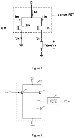
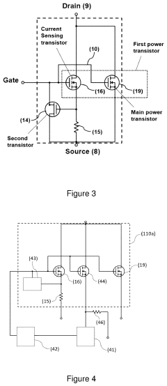
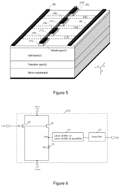
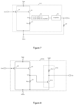
Current sensing in power semiconductor devices
PatentPendingUS20240162224A1
Innovation
- A heterojunction III-nitride high voltage/power device with a main power transistor, a sensing transistor, a resistive sensing load, and an amplifier structure that includes a level shifter and a differential amplifier, where the sensing transistor has a similar architecture to the main power transistor but with a scaled-down area or gate perimeter, and the amplifier structure provides a low VCS signal to improve linearity and accuracy while maintaining high sensitivity.
Thermal Management Considerations
Thermal management is a critical consideration when implementing GaN power devices with high-frequency transformers in EMI/EMC-optimized designs. GaN devices operate at significantly higher switching frequencies than traditional silicon-based semiconductors, which while beneficial for reducing magnetic component sizes, introduces substantial thermal challenges that must be addressed systematically.
The inherent characteristics of GaN devices create unique thermal management requirements. Their smaller die size results in higher power density, concentrating heat generation in smaller areas. Additionally, the faster switching speeds produce more concentrated thermal spikes during switching transitions. When coupled with high-frequency transformers, these thermal issues become more complex due to core losses and winding losses that increase with frequency.
Effective thermal management strategies must begin at the component level. GaN devices require carefully designed thermal pads with minimal thermal resistance. Direct bonded copper (DBC) substrates or insulated metal substrates (IMS) are preferred for their superior thermal conductivity. The thermal interface materials (TIMs) between the GaN device and heatsink must be selected with particular attention to thermal conductivity and long-term reliability under thermal cycling conditions.
For high-frequency transformers, core material selection becomes paramount. Materials like Mn-Zn ferrites or nanocrystalline cores offer better performance at high frequencies but have different thermal characteristics that must be accounted for in the thermal design. Litz wire configurations in transformer windings help mitigate skin effect losses but may impede heat dissipation if not properly designed with thermal considerations in mind.
System-level thermal management approaches include active cooling solutions such as forced-air cooling or liquid cooling for high-power applications. Thermal simulation tools have become essential in predicting hotspots and optimizing heat flow paths before physical prototyping. These simulations must account for the unique thermal profiles of GaN switching events and high-frequency magnetic components operating simultaneously.
Temperature monitoring and protection circuits are particularly important for GaN-based designs. The implementation of multiple temperature sensors at critical points, coupled with intelligent thermal management algorithms, can prevent thermal runaway conditions. Dynamic frequency adjustment and load-dependent switching strategies can be employed to maintain optimal thermal conditions during operation.
The thermal design must also consider EMI/EMC implications. Heatsinks and thermal structures can act as antennas for radiated emissions if not properly grounded. Conversely, EMI mitigation techniques like shielding can impede thermal dissipation if not carefully integrated into the overall thermal management strategy.
Standards Compliance and Testing Methodologies
Compliance with EMI/EMC standards is critical for GaN power devices with high-frequency transformers, as these components operate at switching frequencies that can generate significant electromagnetic interference. The regulatory landscape includes several key standards that manufacturers must adhere to, including IEC 61000 series for electromagnetic compatibility, CISPR standards for radio disturbance characteristics, and region-specific regulations such as FCC Part 15 in the United States and EN 55011/55022 in Europe.
Testing methodologies for GaN-based power systems require specialized approaches due to the unique characteristics of wide-bandgap semiconductors. Conducted emissions testing typically involves line impedance stabilization networks (LISN) to measure noise conducted back onto power lines, with measurements taken across a frequency range of 150 kHz to 30 MHz. For GaN devices operating at high frequencies, extended testing up to 100 MHz may be necessary to capture higher-order harmonics.
Radiated emissions testing requires anechoic or semi-anechoic chambers to measure electromagnetic fields generated by the device under test. The fast switching speeds of GaN devices (often <10ns) create significant high-frequency content that demands careful measurement techniques. Near-field probing has emerged as a valuable diagnostic tool during development phases, allowing engineers to identify specific emission sources within the circuit layout.
Immunity testing represents another critical aspect of EMC compliance, ensuring that GaN power systems can operate reliably in electromagnetically noisy environments. Standard tests include electrostatic discharge (ESD) immunity, electrical fast transient (EFT) immunity, surge immunity, and radiated/conducted RF immunity. The high operating frequencies of GaN devices can sometimes make them more susceptible to certain types of interference, necessitating robust design practices.
Pre-compliance testing has become increasingly important in the development cycle for GaN-based power systems. This approach involves performing preliminary EMI/EMC assessments during the prototype phase using simplified test setups. While not a replacement for full compliance testing, these early evaluations can identify potential issues before designs are finalized, reducing costly redesign cycles.
The testing process should follow a systematic methodology: initial pre-compliance screening, design optimization based on findings, verification testing, and finally full compliance certification. Documentation of test results must be comprehensive, including test setups, measurement conditions, and detailed performance data across all required frequency ranges and operating modes.
Unlock deeper insights with Patsnap Eureka Quick Research — get a full tech report to explore trends and direct your research. Try now!
Generate Your Research Report Instantly with AI Agent
Supercharge your innovation with Patsnap Eureka AI Agent Platform!