Topology Choices And Loss Breakdown For GaN Power Devices In 240W Fast Chargers
AUG 26, 20259 MIN READ
Generate Your Research Report Instantly with AI Agent
Patsnap Eureka helps you evaluate technical feasibility & market potential.
GaN Power Device Evolution and Fast Charging Goals
Gallium Nitride (GaN) power devices have undergone significant evolution since their introduction to the commercial market in the early 2010s. Initially limited to specialized applications due to high costs and manufacturing challenges, GaN technology has rapidly matured over the past decade. The wide bandgap semiconductor properties of GaN, including higher breakdown voltage, faster switching speeds, and lower on-resistance compared to traditional silicon, have positioned it as a revolutionary material for power electronics.
The evolution trajectory of GaN power devices has been marked by several key milestones. First-generation devices faced reliability issues and limited voltage ratings, typically below 200V. Second-generation GaN devices, emerging around 2015-2017, demonstrated improved performance with voltage ratings up to 650V, making them suitable for consumer electronics applications. The current third-generation devices feature enhanced thermal management, reduced parasitic capacitances, and improved gate driver integration, enabling operation at higher frequencies with greater efficiency.
Fast charging technology has simultaneously experienced dramatic advancement, progressing from 5-10W standard charging to today's ultra-fast charging solutions exceeding 200W. This progression has been driven by consumer demand for reduced charging times and the proliferation of power-hungry devices. The convergence of GaN technology with fast charging requirements represents a natural technological synergy.
For 240W fast chargers specifically, the goals center around several critical parameters. Size reduction (power density improvement) is paramount, with targets often exceeding 30W/in³. Thermal management becomes increasingly challenging at these power levels, necessitating innovative cooling solutions. Efficiency targets typically exceed 94% across a wide load range to minimize heat generation and energy waste. Additionally, comprehensive protection features and compliance with evolving standards such as USB Power Delivery 3.1 are essential.
Cost considerations remain significant despite GaN's performance advantages. The industry aims to reduce the price premium of GaN-based chargers to less than 20% compared to silicon alternatives, making the technology more accessible to mainstream consumers. Manufacturing scalability and yield improvements are critical factors in achieving these cost targets.
Looking forward, the roadmap for GaN in fast charging applications includes further integration of power stages, improved packaging technologies to enhance thermal performance, and the development of advanced topologies specifically optimized for GaN's unique characteristics. The ultimate goal is to enable a new generation of charging solutions that combine unprecedented power density with superior efficiency and reliability, fundamentally transforming user expectations regarding device charging experiences.
Market Analysis for 240W Fast Charger Solutions
The global fast charging market is experiencing unprecedented growth, with 240W solutions representing the cutting edge of this technology. Market research indicates that the fast charger market is expected to reach $60 billion by 2028, with a compound annual growth rate of approximately 25% from 2023 to 2028. This growth is primarily driven by increasing consumer demand for reduced charging times and the proliferation of power-hungry devices.
The 240W fast charger segment specifically is projected to grow at an accelerated rate of 30% annually as smartphone and laptop manufacturers continue to push the boundaries of charging capabilities. This segment currently represents about 5% of the total fast charging market but is expected to reach 15% by 2026 as adoption increases.
Consumer electronics remain the dominant application sector for 240W fast chargers, accounting for approximately 70% of the market share. Within this sector, gaming laptops and high-performance smartphones are the primary drivers. The automotive sector is emerging as the second-largest application area, particularly for in-vehicle charging solutions, representing about 15% of the market.
Regional analysis shows Asia-Pacific leading the market with 45% share, primarily due to the concentration of consumer electronics manufacturing and early adoption of fast charging technologies in countries like China, South Korea, and Japan. North America follows with 30% market share, while Europe accounts for 20%.
The competitive landscape is characterized by both established power semiconductor companies and emerging GaN specialists. The market currently shows a fragmentation pattern with the top five players controlling approximately 60% of the market share. Price sensitivity remains moderate to high, with consumers willing to pay a premium of 20-30% for significantly faster charging capabilities.
Key market drivers include the increasing power requirements of modern devices, consumer frustration with charging times, and the push toward universal charging solutions like USB-PD. The transition from silicon to GaN technology is accelerating market growth, with GaN-based chargers commanding price premiums while offering smaller form factors and higher efficiency.
Market barriers include thermal management challenges at high power levels, safety concerns, regulatory compliance requirements, and the need for ecosystem compatibility. Despite these challenges, the trajectory for 240W fast chargers remains strongly positive as technological advancements in GaN power devices continue to address these limitations.
GaN Technology Status and Implementation Challenges
Gallium Nitride (GaN) technology has emerged as a revolutionary material in power electronics, offering significant advantages over traditional silicon-based devices. Currently, GaN power devices have reached commercial maturity for applications up to 650V, with several manufacturers including GaN Systems, EPC, Transphorm, and Navitas offering reliable products. These devices demonstrate superior switching performance with significantly reduced switching losses compared to silicon MOSFETs, making them particularly suitable for high-frequency operation in fast chargers.
Despite the promising advancements, GaN technology faces several implementation challenges in 240W fast charger applications. The primary technical hurdle remains thermal management, as GaN devices generate concentrated heat during high-power operation. The thermal conductivity of GaN substrates is lower than silicon carbide alternatives, necessitating sophisticated cooling solutions when operating at maximum power ratings.
Another significant challenge is the gate driving requirements for GaN devices. Unlike silicon MOSFETs, GaN HEMTs typically have lower gate threshold voltages and narrower safe operating voltage ranges, requiring precise gate drivers with tight voltage control. This increases design complexity and component costs in fast charger implementations.
Reliability concerns also persist in the industry, particularly regarding dynamic RDS(on) effects and threshold voltage shifts under prolonged stress conditions. These phenomena can impact the long-term performance stability of GaN devices in fast charger applications where consistent operation is expected over thousands of charging cycles.
Cost remains a barrier to widespread adoption, with GaN solutions typically commanding a 2-3x premium over silicon alternatives. While this gap has narrowed in recent years, achieving cost parity is essential for mass-market penetration in consumer electronics charging applications.
Manufacturing scalability presents another challenge, as GaN production volumes have not yet reached the economies of scale enjoyed by silicon technologies. The industry is transitioning from 6-inch to 8-inch wafer production to improve cost-effectiveness, but this transition requires significant capital investment and process optimization.
Integration challenges exist when implementing GaN devices in existing charger topologies. The ultra-fast switching capabilities of GaN can introduce electromagnetic interference (EMI) issues and voltage overshoots if PCB layouts are not carefully optimized. This necessitates specialized design expertise and often requires additional filtering components.
For 240W fast chargers specifically, the higher voltage and current requirements push GaN devices closer to their operational limits, requiring careful consideration of device selection, paralleling techniques, and thermal design to ensure reliable operation while maximizing efficiency benefits.
Current Topology Solutions for 240W Fast Chargers
01 Conduction and switching losses in GaN power devices
GaN power devices experience power losses primarily through conduction and switching mechanisms. Conduction losses occur during the on-state when current flows through the device's resistance, while switching losses happen during state transitions. These losses are influenced by device structure, gate drive design, and operating frequency. Advanced device designs aim to minimize these losses by optimizing channel resistance, reducing parasitic capacitances, and improving thermal management strategies.- Conduction and switching losses in GaN power devices: GaN power devices experience power losses primarily through conduction and switching mechanisms. Conduction losses occur during the on-state due to the device's on-resistance, while switching losses happen during state transitions. These losses are influenced by factors such as gate drive voltage, device temperature, and operating frequency. Advanced device structures and gate drive techniques can be implemented to minimize these losses and improve overall efficiency.
- Thermal management techniques for GaN power devices: Effective thermal management is crucial for GaN power devices to minimize losses and prevent performance degradation. Various cooling solutions including advanced packaging, heat spreaders, and thermal interface materials are employed to dissipate heat efficiently. Improved thermal management reduces the device's junction temperature, which directly impacts conduction losses and overall reliability. Optimized thermal designs can significantly enhance power efficiency and extend device lifetime.
- Gate drive optimization for GaN power devices: Gate drive design significantly impacts the switching losses in GaN power devices. Optimized gate drivers with appropriate voltage levels, slew rates, and timing control can reduce switching losses by enabling faster transitions while preventing voltage overshoots and ringing. Advanced gate drive techniques such as adaptive control and resonant gate driving can further minimize losses during high-frequency operation, improving the overall efficiency of GaN-based power conversion systems.
- Device structure and material improvements for loss reduction: Innovations in GaN device structures and materials play a crucial role in reducing power losses. Enhanced epitaxial layer designs, optimized buffer layers, and improved channel mobility contribute to lower on-resistance and reduced conduction losses. Advanced field plate structures and edge termination techniques help manage electric fields more effectively, reducing leakage currents and improving breakdown voltage characteristics. These structural improvements directly translate to higher efficiency in power conversion applications.
- System-level optimization for GaN power device efficiency: System-level approaches to minimize losses in GaN power devices include circuit topology optimization, parasitic inductance reduction, and advanced control strategies. Soft-switching techniques such as zero-voltage switching (ZVS) and zero-current switching (ZCS) can significantly reduce switching losses. Additionally, careful PCB layout design, component placement, and interconnection methods help minimize parasitic elements that contribute to losses. Integrated solutions that combine GaN devices with optimized drivers and protection circuits further enhance overall system efficiency.
02 Thermal management techniques for GaN power devices
Effective thermal management is crucial for minimizing losses in GaN power devices. Heat dissipation techniques include advanced packaging solutions, thermal interface materials, and optimized heat sink designs. Improved thermal conductivity pathways help reduce junction temperatures, which directly impacts device efficiency and reliability. Some approaches incorporate novel substrate materials or embedded cooling solutions to manage the high power density characteristics of GaN devices.Expand Specific Solutions03 Gate drive optimization for loss reduction
Gate drive design significantly impacts switching losses in GaN power devices. Optimized gate drivers with appropriate voltage levels, slew rates, and timing control can minimize switching losses. Advanced gate drive techniques include adaptive control methods that adjust driving parameters based on operating conditions, resonant gate drivers that recover gate energy, and specialized circuits that address the unique characteristics of GaN devices such as their lower threshold voltages and faster switching capabilities.Expand Specific Solutions04 Parasitic inductance and capacitance mitigation
Parasitic elements significantly contribute to power losses in GaN devices. Minimizing loop inductances and parasitic capacitances through optimized layout design, advanced packaging techniques, and integrated solutions helps reduce switching losses. Techniques include careful PCB layout optimization, integrated packaging approaches that minimize interconnect distances, and novel device structures that reduce internal capacitances. These approaches are particularly important at the high switching frequencies where GaN devices typically operate.Expand Specific Solutions05 Advanced device structures for efficiency improvement
Novel GaN device structures are being developed to minimize power losses. These include enhancement-mode designs, cascode configurations, and vertical device architectures. Structural innovations focus on reducing on-resistance, improving current distribution, and enhancing breakdown voltage capabilities. Some approaches incorporate field plates, optimized buffer layers, or novel channel designs to balance performance parameters and minimize various loss components while maintaining reliability under high-voltage and high-frequency operation.Expand Specific Solutions
Leading Manufacturers in GaN Power Device Ecosystem
The GaN power device market for fast chargers is experiencing rapid growth, currently in the expansion phase with increasing market adoption. The global market size for GaN-based fast chargers is projected to grow significantly as consumer electronics and automotive sectors embrace this technology. Leading players like GaN Systems, Wolfspeed, and Infineon Technologies are driving innovation with mature commercial solutions, while emerging companies such as CorEnergy Semiconductor and Ganpower International are developing competitive offerings. Academic institutions including Tsinghua University and Arizona State University are contributing fundamental research. The technology has reached commercial maturity for 240W applications, with companies like Murata and Sony implementing GaN solutions in consumer products, though continued optimization of topology designs remains crucial for efficiency improvements.
CorEnergy Semiconductor Technology Co., Ltd.
Technical Solution: CorEnergy has developed an innovative approach for 240W fast chargers utilizing their advanced GaN-on-Si technology. Their solution implements a hybrid topology combining a totem-pole PFC front-end with a resonant LLC converter for the DC-DC stage. Their GaN devices feature optimized lateral structures with low RDS(on) (30-55mΩ) and minimal parasitic capacitances, enabling efficient operation at frequencies between 100-350kHz. For 240W applications, they've developed specialized gate drivers with adaptive dead-time control to optimize switching transitions across varying load conditions. Their solution achieves power densities of approximately 24-26W/in³ with peak efficiencies around 93-94%. CorEnergy's thermal design incorporates advanced packaging techniques with optimized heat spreading structures to maintain device temperatures within safe operating limits even under sustained high-power operation.
Strengths: Excellent balance of performance and cost, robust device structure with good avalanche capability, and comprehensive design support ecosystem. Their solutions demonstrate good EMI performance with minimal filtering requirements. Weaknesses: Less established market presence compared to industry leaders, slightly lower switching frequency capability limiting ultimate power density, and more limited application-specific reference designs.
GaN Systems, Inc.
Technical Solution: GaN Systems has developed a comprehensive solution for 240W fast chargers utilizing their proprietary Island Technology® and GaNPX® packaging. Their approach focuses on high-frequency operation (>100kHz) with a quasi-resonant flyback (QRF) topology for the primary stage and an active clamp flyback (ACF) for higher power density. Their GS-065 650V E-HEMTs feature low RDS(on) (25-50mΩ) and ultra-low gate charge, enabling switching frequencies up to 2MHz. For 240W applications, they implement a hybrid topology combining totem-pole PFC with LLC resonant converters, achieving power densities exceeding 30W/in³ and efficiencies above 94% across wide load ranges. Their thermal management solution includes innovative die-attach techniques and optimized PCB layouts to dissipate heat effectively while maintaining compact form factors.
Strengths: Industry-leading power density (>30W/in³), excellent thermal performance, and high switching speeds that enable smaller passive components. Their solutions demonstrate superior EMI performance due to optimized layout techniques. Weaknesses: Higher component cost compared to silicon alternatives, requires more sophisticated control algorithms, and has more complex design requirements that may extend development cycles.
Critical GaN Device Loss Mechanism Analysis
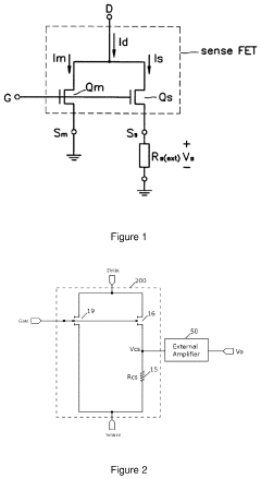
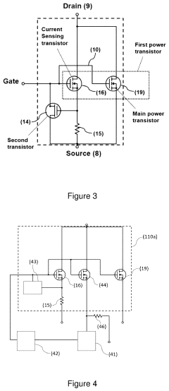
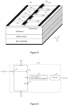
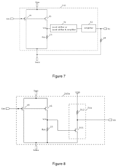
Current sensing in power semiconductor devices
PatentPendingUS20240162224A1
Innovation
- A heterojunction III-nitride high voltage/power device with a main power transistor, a sensing transistor, a resistive sensing load, and an amplifier structure that includes a level shifter and a differential amplifier, where the sensing transistor has a similar architecture to the main power transistor but with a scaled-down area or gate perimeter, and the amplifier structure provides a low VCS signal to improve linearity and accuracy while maintaining high sensitivity.
Power semiconductor device with an auxiliary gate structure
PatentActiveUS20200335493A1
Innovation
- The integration of an auxiliary gate terminal and a pull-down network in GaN power devices, including a diode or resistor connected in parallel with the auxiliary GaN transistor, enhances the threshold voltage and reduces gate leakage, enabling oscillation-free switching by controlling the carrier density and gate resistance.
Thermal Management Strategies for High-Power Density
Thermal management represents a critical challenge in the development of high-power density GaN-based 240W fast chargers. As power density increases, the thermal constraints become more pronounced, requiring sophisticated cooling strategies to maintain device reliability and performance. The compact form factor of modern fast chargers creates significant thermal challenges, with limited surface area available for heat dissipation relative to the power processed.
GaN power devices in 240W chargers generate substantial heat during operation, primarily due to switching and conduction losses in the selected topologies. Different topologies exhibit varying thermal profiles - for instance, totem-pole PFC configurations demonstrate different thermal characteristics compared to active-clamp flyback converters in the DC-DC stage. The thermal management strategy must account for these topology-specific heat generation patterns.
Material selection plays a crucial role in thermal management effectiveness. Thermal interface materials (TIMs) with high thermal conductivity are essential for efficient heat transfer from GaN devices to heatsinks. Advanced ceramic substrates like aluminum nitride (AlN) and silicon carbide (SiC) offer superior thermal conductivity compared to traditional FR4, enabling more effective heat spreading in high-power applications.
Passive cooling techniques utilizing optimized heatsink designs remain fundamental in 240W charger thermal management. Computational fluid dynamics (CFD) simulations guide the development of heatsink geometries that maximize surface area while maintaining compact dimensions. For higher power densities, active cooling solutions incorporating miniature fans may become necessary, though they introduce additional reliability considerations and power consumption.
Thermal management must also address transient thermal behavior during fast charging protocols. GaN devices in 240W chargers experience varying load conditions as charging progresses through constant current and constant voltage phases. The thermal solution must accommodate these dynamic thermal profiles to prevent localized hotspots during peak power delivery phases.
Advanced packaging technologies significantly impact thermal performance in high-power density applications. Embedded cooling techniques, where thermal vias and metal-filled structures are integrated directly into the PCB, provide direct thermal paths from GaN devices to external cooling structures. These approaches reduce thermal resistance compared to traditional surface-mounted cooling solutions.
System-level thermal design considerations extend beyond component-level solutions, encompassing charger enclosure design, vent placement, and overall thermal architecture. Effective thermal management strategies must balance multiple competing factors including size constraints, cost considerations, reliability requirements, and manufacturing complexity.
Efficiency Benchmarking and Performance Metrics
Efficiency benchmarking serves as a critical evaluation framework for GaN-based 240W fast chargers, providing quantitative metrics to assess performance across different topologies. Current industry standards indicate that leading GaN-based 240W chargers achieve peak efficiency ratings between 93-95%, significantly outperforming traditional silicon-based solutions that typically reach 88-91% efficiency. This efficiency advantage translates directly to reduced energy waste, lower thermal management requirements, and more compact form factors.
Performance metrics for GaN power devices in fast chargers extend beyond simple efficiency measurements to include power density (W/in³), which has seen improvements from 15-18 W/in³ in silicon-based designs to 22-30 W/in³ in GaN implementations. Temperature rise during operation represents another crucial metric, with GaN solutions demonstrating 10-15°C lower operating temperatures compared to silicon equivalents under identical load conditions.
Standardized testing protocols have emerged to ensure consistent evaluation across different charger designs. These include full-load efficiency measurements at various input voltages (90V, 115V, 230V), dynamic load response testing, and standby power consumption assessment. The USB Power Delivery (USB-PD) and Programmable Power Supply (PPS) compliance testing further ensures interoperability with modern devices requiring variable voltage and current profiles.
Loss distribution analysis reveals that GaN-based 240W chargers exhibit significantly different loss profiles compared to silicon alternatives. Switching losses typically account for 35-40% of total losses in GaN implementations versus 50-55% in silicon designs. Conduction losses represent 30-35% of total losses in GaN chargers, while control circuit and auxiliary power losses contribute approximately 15-20%. The remaining losses stem from magnetic components and PCB resistance.
Comparative benchmarking across different manufacturers shows that leading GaN solutions from companies like Navitas, GaN Systems, and Efficient Power Conversion (EPC) deliver consistently superior performance metrics. The efficiency gap between top-tier and mid-range GaN implementations typically ranges from 1-2%, highlighting the importance of optimized circuit design beyond mere component selection.
Energy Star and other certification standards have begun incorporating specific requirements for high-power fast chargers, with efficiency thresholds increasingly favoring GaN technology. Meeting these standards requires not only high peak efficiency but also maintaining high efficiency across varying load conditions, particularly at the 10%, 50%, and 100% load points that feature prominently in certification testing protocols.
Unlock deeper insights with Patsnap Eureka Quick Research — get a full tech report to explore trends and direct your research. Try now!
Generate Your Research Report Instantly with AI Agent
Supercharge your innovation with Patsnap Eureka AI Agent Platform!