System-Level Cost Reduction With GaN Power Devices: Magnetics And Heatsinks
AUG 26, 20259 MIN READ
Generate Your Research Report Instantly with AI Agent
Patsnap Eureka helps you evaluate technical feasibility & market potential.
GaN Power Technology Evolution and Objectives
Gallium Nitride (GaN) power technology has undergone significant evolution since its initial development in the early 1990s. Originally conceived for RF applications in defense and telecommunications, GaN has progressively transitioned into power electronics due to its superior material properties compared to silicon. The wide bandgap characteristics of GaN enable higher breakdown voltages, faster switching speeds, and lower on-resistance, making it particularly suitable for high-frequency, high-power applications.
The evolution of GaN power technology can be traced through several key developmental phases. The first phase (1990-2005) focused primarily on material science challenges, addressing issues such as substrate compatibility, defect density reduction, and basic device structures. During this period, researchers concentrated on establishing fundamental fabrication techniques and understanding the unique properties of GaN semiconductors.
The second phase (2005-2015) marked the transition from laboratory research to initial commercialization efforts. This period saw significant improvements in device reliability, the development of enhanced GaN-on-Si technology to reduce costs, and the introduction of the first commercial GaN power transistors. Companies like EPC, Transphorm, and GaN Systems emerged as pioneers in bringing GaN power devices to market.
The current phase (2015-present) represents the maturation and broader adoption of GaN technology across multiple industries. Enhanced manufacturing processes have led to improved yield rates and reduced costs, while device performance continues to advance with innovations in packaging, gate structures, and integration capabilities. The focus has shifted toward system-level optimization, particularly in areas such as magnetics and thermal management.
The primary objectives of GaN power technology development now center on achieving comprehensive system-level cost reductions while maintaining or enhancing performance advantages. This includes optimizing power density to reduce the size of magnetic components, improving thermal efficiency to minimize heatsink requirements, and enhancing integration capabilities to reduce overall system complexity and component count.
Looking forward, the technology roadmap aims to further reduce costs through economies of scale, improved manufacturing processes, and innovative system designs that fully leverage GaN's unique capabilities. The ultimate goal is to position GaN as the dominant technology for medium-voltage (100V-900V) power applications, offering superior efficiency, size, and cost metrics compared to both silicon and silicon carbide alternatives in specific application segments.
Industry projections suggest that achieving these objectives could expand the GaN power device market from approximately $1 billion in 2023 to over $5 billion by 2030, representing a significant shift in the power semiconductor landscape and enabling new generations of more efficient power conversion systems across multiple sectors.
Market Analysis for GaN-Based Power Solutions
The global power electronics market is experiencing a significant shift towards Gallium Nitride (GaN) technology, with the GaN power device market projected to reach $1.75 billion by 2026, growing at a CAGR of approximately 35% from 2021. This remarkable growth is primarily driven by the superior performance characteristics of GaN compared to traditional silicon-based solutions, particularly in high-frequency and high-power applications.
The demand for GaN-based power solutions is particularly strong in sectors requiring high efficiency and compact designs. Consumer electronics represents the largest market segment, with manufacturers increasingly adopting GaN technology for fast chargers and power adapters. This adoption is evidenced by the proliferation of GaN-based charging solutions from major brands, offering smaller form factors and faster charging capabilities.
Industrial power supplies constitute another significant market segment, where the reduced size of magnetics and heatsinks enabled by GaN technology translates to substantial cost savings and improved power density. The automotive sector, especially electric vehicles, is emerging as a high-growth area for GaN power devices, with applications in onboard chargers and DC-DC converters benefiting from the reduced cooling requirements and smaller magnetic components.
Regionally, Asia-Pacific dominates the GaN power device market, accounting for approximately 45% of global demand. This dominance is attributed to the strong presence of consumer electronics manufacturing and the aggressive adoption of new technologies in countries like China, Japan, and South Korea. North America follows with roughly 30% market share, driven by early adoption in industrial and defense applications.
The system-level cost benefits of GaN technology are becoming increasingly recognized across industries. While the unit cost of GaN devices remains higher than silicon alternatives, the total system cost often proves more favorable when considering the reduced size and cost of passive components, particularly magnetics and heatsinks. Market analysis indicates that systems utilizing GaN can achieve 15-25% overall cost reduction compared to silicon-based designs when factoring in these system-level savings.
Market forecasts suggest that as GaN manufacturing scales and technology matures, the price premium over silicon will continue to decrease, further accelerating adoption. The compound annual price reduction for GaN power devices is estimated at 10-15%, significantly outpacing the 3-5% typical for mature silicon devices. This trend is expected to expand GaN's addressable market substantially over the next five years.
GaN Power Devices: Current Limitations and Challenges
Despite the significant advantages of Gallium Nitride (GaN) power devices in system-level cost reduction, particularly in magnetics and heatsink applications, several technical limitations and challenges persist that hinder their widespread adoption. The wide bandgap semiconductor technology faces material-related challenges, including defect densities in GaN epitaxial layers that can compromise device reliability and performance. Crystal dislocations and point defects in the GaN material structure continue to impact yield rates and long-term stability of these devices.
Thermal management remains a critical challenge for GaN power devices. While they can operate at higher temperatures than silicon counterparts, the thermal conductivity of GaN substrates is still lower than ideal, creating localized hotspots that can degrade performance and reliability. The thermal interface between GaN devices and cooling systems requires sophisticated solutions to effectively dissipate heat, especially in high-power density applications.
Dynamic RDS(on) degradation presents another significant limitation. Under high-voltage switching conditions, GaN devices experience an increase in on-resistance over time, which can reduce efficiency and affect system performance. This phenomenon, attributed to charge trapping mechanisms, requires careful consideration in circuit design and thermal management strategies.
Gate driving complexity poses substantial implementation challenges. GaN devices typically require more precise gate drive voltages compared to silicon MOSFETs, with narrower operating margins. The gate drive circuitry must be carefully designed to prevent false triggering and ensure reliable operation, adding complexity to the overall system design.
Packaging technology limitations also impact GaN device performance. Current packaging solutions often fail to fully leverage GaN's high-frequency capabilities due to parasitic inductances and capacitances. Advanced packaging techniques are needed to minimize these parasitics and maximize the switching speed advantages of GaN.
Electromagnetic interference (EMI) management becomes more challenging with GaN's faster switching speeds. The rapid voltage and current transitions generate higher frequency electromagnetic emissions that require sophisticated filtering and shielding solutions, potentially offsetting some of the size advantages gained through higher operating frequencies.
Reliability and qualification standards for GaN devices are still evolving. The industry lacks standardized qualification procedures specifically tailored for GaN technology, creating uncertainty for system designers and slowing adoption in mission-critical applications. Long-term reliability data remains limited compared to mature silicon technologies.
Cost factors continue to present barriers to widespread adoption. While system-level cost benefits can be realized through reduced magnetics and heatsink requirements, the unit cost of GaN devices remains higher than silicon alternatives. Manufacturing processes have not yet achieved the economies of scale necessary to drive costs down to competitive levels for all application segments.
System-Level Cost Optimization Strategies for GaN Implementation
01 Substrate and Epitaxial Growth Optimization
Cost reduction in GaN power devices can be achieved through optimizing substrate materials and epitaxial growth processes. This includes using silicon substrates instead of more expensive materials like silicon carbide or sapphire, developing improved buffer layers to manage stress and defects, and implementing more efficient growth techniques that reduce material waste and processing time while maintaining device performance.- Substrate and Epitaxial Growth Optimization: Cost reduction in GaN power devices can be achieved through optimizing substrate materials and epitaxial growth processes. This includes using silicon substrates instead of more expensive materials like sapphire or silicon carbide, developing improved buffer layers to manage stress, and implementing more efficient growth techniques that reduce material waste and processing time. These approaches help lower the material costs while maintaining device performance.
- Advanced Manufacturing Techniques: Implementation of advanced manufacturing techniques can significantly reduce the production costs of GaN power devices. These include batch processing methods, automated assembly lines, and improved wafer handling systems. Additionally, techniques such as wafer bonding, selective area growth, and optimized lithography processes can increase yield rates and reduce processing steps, leading to overall cost reduction in manufacturing.
- Device Structure Simplification: Simplifying the structure of GaN power devices can lead to cost reduction by minimizing the number of processing steps and materials required. This includes developing vertical device architectures that require fewer masks and lithography steps, implementing innovative gate designs that reduce complexity, and creating more efficient device layouts that maximize the number of devices per wafer. These structural optimizations maintain electrical performance while reducing manufacturing costs.
- Integration and Packaging Innovations: Innovations in integration and packaging technologies can reduce the overall cost of GaN power devices. This includes developing monolithic integration approaches that combine multiple components on a single chip, implementing advanced packaging techniques that improve thermal management without expensive materials, and creating standardized packaging solutions that reduce assembly costs. These innovations help decrease the total system cost while maintaining reliability.
- Supply Chain and Production Scale Optimization: Optimizing the supply chain and increasing production scale can significantly reduce the cost of GaN power devices. This includes establishing strategic partnerships with material suppliers, implementing economies of scale through larger wafer sizes and higher volume production, standardizing processes across different device types, and developing more efficient testing methodologies. These approaches help reduce overhead costs and increase manufacturing efficiency.
02 Advanced Packaging and Integration Techniques
Innovative packaging and integration methods can significantly reduce the overall cost of GaN power devices. These techniques include wafer-level packaging, chip-scale packaging, and advanced assembly methods that minimize the use of expensive materials. Integration of multiple components into single packages and the development of more efficient thermal management solutions also contribute to cost reduction while maintaining or improving device performance.Expand Specific Solutions03 Manufacturing Process Improvements
Enhancements in manufacturing processes play a crucial role in reducing GaN power device costs. This includes implementing automated production lines, developing more efficient cleaning and etching processes, optimizing lithography techniques, and reducing the number of processing steps. Process yield improvements through better quality control and defect management also contribute significantly to overall cost reduction.Expand Specific Solutions04 Device Structure and Design Optimization
Innovative device structures and designs can reduce manufacturing costs while maintaining or improving performance. This includes simplified device architectures that require fewer processing steps, optimized gate designs that improve yield, and novel device topologies that use less material. Reducing device dimensions while maintaining performance characteristics also contributes to cost efficiency through increased die per wafer.Expand Specific Solutions05 Supply Chain and Scale Optimization
Economies of scale and supply chain optimization are critical for reducing GaN power device costs. This includes developing strategic partnerships with material suppliers, implementing volume production techniques, standardizing device specifications to increase production volumes, and establishing efficient testing and qualification procedures. Vertical integration of the manufacturing process can also lead to significant cost reductions by eliminating markup between production stages.Expand Specific Solutions
Leading Manufacturers and Competitors in GaN Industry
The GaN power device market for system-level cost reduction in magnetics and heatsinks is currently in a growth phase, with an expanding market size driven by efficiency demands in power electronics. The technology has reached moderate maturity, with key players advancing commercial applications while continuing R&D efforts. Leading companies like GaN Systems and Navitas Semiconductor have established strong positions in GaN power IC development, while major electronics manufacturers including Samsung, Huawei, and NXP are integrating these solutions into their product ecosystems. Research institutions such as Zhejiang University and Southeast University collaborate with industry partners to overcome remaining technical challenges. The competitive landscape features both specialized GaN-focused companies and diversified semiconductor giants competing to optimize system-level benefits through reduced size and weight of magnetic components and heatsinks.
GaN Systems, Inc.
Technical Solution: GaN Systems has developed a comprehensive approach to system-level cost reduction using GaN power devices, focusing on both magnetic components and thermal management. Their GaN E-HEMT (Enhancement-mode High Electron Mobility Transistor) technology enables operation at switching frequencies 3-10 times higher than traditional silicon devices, allowing for significant reduction in magnetic component size. Their designs incorporate planar magnetics that reduce core losses by up to 70% compared to conventional designs. For thermal management, GaN Systems has pioneered bottom-side cooling techniques that eliminate the need for bulky heatsinks by utilizing the PCB as a thermal dissipation path. Their Island Technology® packaging provides superior thermal performance with junction-to-case thermal resistance as low as 0.5°C/W, enabling up to 67% reduction in heatsink size. The company has demonstrated power density improvements of over 3x in various applications including power supplies, motor drives, and automotive systems.
Strengths: Industry-leading power density achievements; comprehensive design ecosystem including reference designs and simulation tools; patented packaging technology optimized for thermal performance. Weaknesses: Higher initial component cost compared to silicon alternatives; requires redesign of existing systems to fully leverage benefits; thermal management advantages diminish in extremely high-power applications.
NexGen Power Systems, Inc.
Technical Solution: NexGen Power Systems has developed a vertical GaN technology platform specifically addressing system-level cost reduction through magnetic and thermal optimization. Their approach utilizes native GaN substrates rather than traditional silicon or silicon carbide substrates, enabling higher breakdown voltages (up to 1200V) while maintaining superior switching performance. NexGen's vertical GaN architecture allows for switching frequencies exceeding 1MHz with minimal switching losses, enabling magnetic components to be reduced by up to 80% in volume. Their technology incorporates innovative thermal management solutions including direct substrate cooling that reduces thermal resistance by approximately 40% compared to lateral GaN devices. NexGen has demonstrated power supplies with power densities exceeding 1kW/in³ while maintaining high efficiency (>98%) through the combination of reduced magnetic volume and optimized thermal management. Their integrated approach includes custom magnetic designs with low-profile planar transformers and inductors specifically optimized for high-frequency GaN operation.
Strengths: Vertical GaN architecture provides superior thermal performance compared to lateral GaN devices; higher voltage capability enables single-device solutions where cascaded devices were previously required; native GaN substrates offer lower defect density. Weaknesses: Higher manufacturing complexity and cost for native GaN substrates; less established ecosystem compared to other GaN providers; limited production volume capability currently constrains widespread adoption.
Magnetics and Thermal Management Innovations for GaN
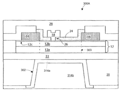
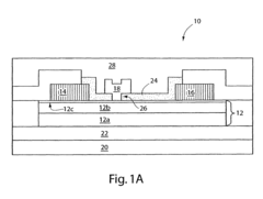
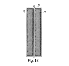
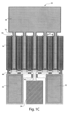
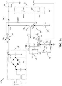
Gallium nitride material devices and thermal designs thereof
PatentActiveUS7745848B1
Innovation
- The design involves arranging transistors in cells with optimized spacing and staggered configurations, along with thermally conductive packaging and selective substrate removal to enhance heat conduction, including the use of vias and thermally conductive material regions to improve thermal resistance.
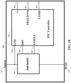
Integrated GAN power devices including PFC and QR flyback controllers
PatentPendingUS20250192670A1
Innovation
- The integration of a Gallium Nitride (GaN) power device with a reduced pin count power factor correction (PFC) controller circuit, enabling co-packaging of the controller IC with the GaN power switch in a semiconductor package, thereby reducing the number of external components and pins.
Supply Chain Considerations for GaN Power Components
The GaN power device supply chain presents unique considerations that significantly impact system-level cost reduction strategies. Current GaN supply chains remain less mature than traditional silicon counterparts, with fewer established suppliers and manufacturing facilities globally. This limited supplier ecosystem creates potential bottlenecks in production scaling and affects component pricing stability, particularly for specialized GaN components optimized for magnetic and thermal system integration.
Primary GaN suppliers include established players like GaN Systems, Efficient Power Conversion (EPC), Transphorm, and Navitas Semiconductor, alongside newer market entrants and divisions of traditional semiconductor manufacturers. Geographic concentration of GaN production facilities presents supply chain vulnerability, with manufacturing primarily centered in East Asia, North America, and select European locations. This concentration increases exposure to regional disruptions and geopolitical tensions.
Raw material considerations also impact GaN supply chains significantly. While gallium is relatively abundant, its extraction as a byproduct of aluminum and zinc processing creates potential supply constraints. Substrate materials for GaN devices, particularly silicon carbide (SiC) wafers, face their own supply limitations that can affect production capacity and component costs.
Manufacturing complexity further influences the GaN supply chain landscape. The specialized processes required for GaN device fabrication, including epitaxial growth techniques and precise doping procedures, limit qualified manufacturing partners. This manufacturing complexity directly impacts yields, production volumes, and ultimately component pricing structures that affect system-level cost calculations.
Qualification and reliability testing requirements add another layer to supply chain considerations. The relatively newer GaN technology requires extensive validation testing, particularly for applications where magnetic and thermal system optimization is critical. These qualification processes extend product development timelines and increase initial costs before system-level savings can be realized.
Inventory management strategies must adapt to GaN supply chain realities. The combination of fewer suppliers, manufacturing complexity, and evolving demand patterns necessitates more sophisticated inventory approaches. System designers must balance just-in-time manufacturing goals with strategic buffer inventories to mitigate supply disruptions that could impact production schedules and overall system costs.
Looking forward, supply chain diversification and vertical integration strategies are emerging as key approaches for managing GaN component availability. Leading power system manufacturers are developing strategic partnerships with GaN suppliers, investing in manufacturing capacity, and exploring alternative sourcing options to ensure stable component supply for optimized magnetic and thermal system designs.
Efficiency and Performance Metrics of GaN-Based Systems
GaN power devices demonstrate superior efficiency metrics compared to traditional silicon-based solutions, with switching losses reduced by up to 80% and conduction losses decreased by approximately 50%. These efficiency improvements directly translate to system-level performance enhancements, particularly in power conversion applications where GaN-based systems consistently achieve efficiency ratings exceeding 98% at high power densities.
Performance evaluation of GaN systems reveals significant advantages in power density metrics, typically achieving 3-4 times higher power density than silicon-based alternatives. This enables more compact designs without compromising thermal performance. Switching frequency capabilities of GaN devices commonly range from 100 kHz to 3 MHz, substantially higher than silicon MOSFETs limited to 100-300 kHz in comparable applications.
The dynamic response characteristics of GaN systems show marked improvements, with slew rates exceeding 100 V/ns and switching transition times below 10 ns. These parameters enable faster transient response in power conversion systems, critical for applications requiring rapid load changes or precise voltage regulation.
Temperature performance metrics indicate GaN devices maintain efficiency advantages across wider temperature ranges, with typical junction temperature ratings of 150°C to 175°C. The positive temperature coefficient of GaN devices provides inherent current sharing capabilities in parallel configurations, enhancing system reliability and thermal management.
Electromagnetic interference (EMI) profiles of GaN-based systems present both challenges and opportunities. While faster switching speeds can increase high-frequency noise, properly designed GaN systems demonstrate reduced EMI footprints due to smaller switching loops and reduced parasitic elements. Measurements show potential EMI reductions of 3-6 dB compared to silicon-based systems with equivalent output power.
Reliability metrics for mature GaN devices now approach or match silicon counterparts, with field failure rates below 10 FIT (failures in time per billion device hours) and projected lifetimes exceeding 15 years in typical operating conditions. This reliability, combined with superior efficiency metrics, establishes GaN technology as increasingly viable for mainstream power applications despite higher initial component costs.
Unlock deeper insights with Patsnap Eureka Quick Research — get a full tech report to explore trends and direct your research. Try now!
Generate Your Research Report Instantly with AI Agent
Supercharge your innovation with Patsnap Eureka AI Agent Platform!